
But things change when you look at the additional cost and complications of converting between the optical and electrical domains. Once those factor into the equation, it’s no surprise why so much data gets forced through serialisers onto electrical traces using an increasingly exotic blend of materials and signal processing.
One indication of how the economics of optical communication affect system design can be seen in the world of data-centre computing. A major trend in this area is to distribute computing across entire rows of server racks. For this, they need to use optical for its long-distance capabilities. But the optical signals do not yet go straight into the switch chips and SoCs on the blades themselves.
”The data-centre customers that we are dealing with, they are still doing optical-electrical conversion on the front panel. They want to take advantage of the optical-module infrastructure that exists,” says Matt Burns, technical marketing manager at connector maker Samtec.
Typically, data-centre operators use pluggable small form-factor (SFP) optical modules based designed to common standards to handle electro-optical conversion. With a wide range of suppliers, the standard modules tend to lead to lower purchase prices and the confidence that the format will be supported for many years.
But pulling in the other direction is the viability of the connection to the board behind that front panel. With earlier generations of serial data link and technologies such as 1Gbit/s Ethernet, it was entirely feasible to route electrical signals through the PCB. But thanks to the advanced transceivers that chipmakers have added to FPGAs and SoCs to support protocols such as PCI Express and 10Gbit/s and 100Gbit/s Ethernet, attempts to use the PCB to link switch chips and SoCs for those signals have run in trouble over signal integrity.
At the Optical Fiber Communication Conference in the spring, Benny Mikkelsen, founder and CTO of Acacia Communications, described a second problem faced by data-centre owners such as Facebook: the amount of front-panel space they need to provide enough optical connections to their compute boards.
Some have had to go to 2U or wider panels simply to provide the area needed for the multiple SFP connectors, even though many have move to quad-density (QSFP) versions. “We can keep putting optics on the front or go to onboard optics or co-packaged optics,” Mikkelsen says.
Tech in its infancy
Today, the technology to bring optical communication to chip packages is still in its infancy, though there are numerous projects underway including an industry-wide research programme: the Integrated Photonic Systems Roadmapping group organised by the International Electronics Manufacturing Initiative (iNEMI). Companies such as Acacia, which is soon to be acquired by Cisco, aims to use 3D stacking based on chiplets to build its next generation of transceivers.
Tom Marrapode, director of advanced technology development in Molex’s optical solutions group, points to power savings of around 30 per cent with fibre to the chip: “The real bang for the buck comes with co-packaged optics. But there are definitely some big technical challenges to solve in in-package or co-packaged optics. The timing on that is maybe around 2025.”
Chips in the 50Tbit/s switch environment could need hundreds of fibre connections. This leads to a mismatch between the way fibre is made today and what will be needed to bring connections down to the package.
Marrapode says it will probably need a combination of wavelength division multiplexing to connect multiple channels over single fibres on top of small-diameter fibres.
“Silicon photonics pitches can be pretty tight: they don’t match today’s fibre. And you will want to move your lasers to a remote position: you can’t have them next to a hot switch-chip package,” he explains. And the connectors will have to make it relatively easy to assemble in a factory though they will not have to be user-connectable as is the case with SFP-type modules.
The question is what happens before the middle of the next decade. The answer depends on the industry. Burns says customers in sectors beyond cloud computing, such as high-end medical and military and aerospace are exploiting mid-board optics. Marrapode notes telecom switch designs have employed the strategy for many years in order to get high-density connections to switch ICs.
The midboard approach uses a connector with built-in electro-optical converters that plugs into a socket placed as close as possible to a serdes transceiver. A flyover fibre from the connector then takes the signal to an optical backplane or pluggable fibre connectors in the front panel. Burns says a common application is to extend protocols such as PCI Express over much longer distances. “We are agnostic in terms of protocols,” Burns notes.
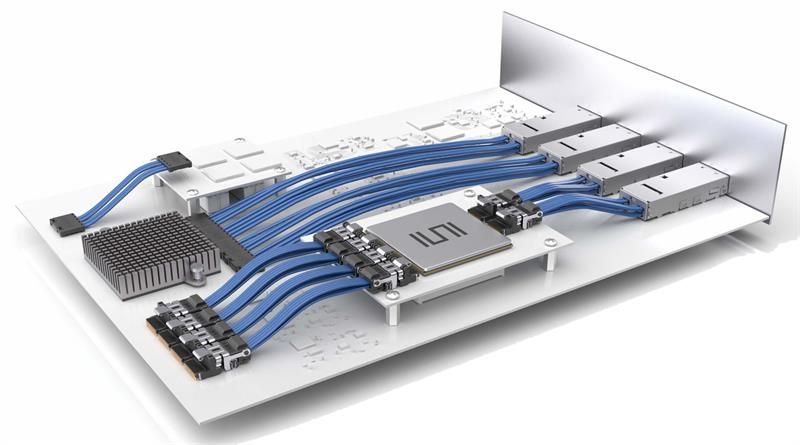
Above: The mid-board approach uses a flyover fibre from the connector to an optical backplane or pluggable fibre connectors
Marrapode says speed is rarely enough on its own to force a move to midboard optics. Instead, the decision is driven largely by the realisation that copper connections will not provide the scalability the system demands. “It’s the point when people say ‘I need optics to get around this whole system’,” he says.
Burns says the military and medical customers have fewer concerns about the multi-sourcing that data-centre customers demand. “They don’t have to be compliant with other vendors.”
For data-centre systems, customers are more willing to stretch the use of front-panel pluggable connectors until they need to move to a replacement for those widely sourced modules.
Marrapode points out that bringing optics to the package will create complications for systems designers.
Ideally, they would want to be able to support a mixture of electrical and optical links to cater for a range of distances, from a few metres to kilometre-level runs. This is straightforward with front-panel pluggable converters, not so with copackaged optics. Vendors may have to provide a selection of boards that provide different combinations.
The arrival of double-density versions of the QSFP connector that co-package multiple transceivers has slowed the growth of the front panel metalwork for the time being. That has been helped by the availability of high-grade flyover cables based on copper twinax wiring and similar approaches. These cables make it possible to take protocols such as 56Gbit/s PAM4 over a distance from an SoC or switch chip to a board’s front panel in situations where routing it through FR4 on a PCB would degrade the signal too much. Products such as Samtec’s Firefly are in the same way as midboard optical connectors but with an electrical connection to conventional front-panel SFP modules.
Marrapode says an additional advantage of twinax flyover cables is that they provide greater flexibility for front-panel design: the cages are no longer constrained by the need to connect to a PCB-based connector. “The twinax flyover is looking really attractive: the performance is good and will probably be the stepping stone to when the photonics go into the switch chip,” he says, adding slightly ruefully: “It’s another push-out for optics. Every speed bump goes through this. It seems there is always something to supplant optics.”
However, the transition may finally be forced on designers when serial links move to 112Gbit/s and the 50Tbit/s switch chip looms, Marrapode adds. There may be no way to stave off direct photonic connection any further. Within five years, the connectors could well be designed for chiplets instead of PCBs and front panels.


