
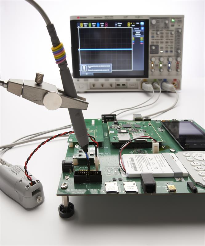
“A probe should have a minimum impact on the probed circuit,” explains Dean Miles, technical marketing manager, EMEA, at Tektronix. “And it needs to be able to maintain adequate signal fidelity for the required measurements. Without that, the result can be wrong or misleading.”
Miles describes the probe as the first link in the measurement chain and, as a result, to be just as important as the oscilloscope itself.
“The entire chain will be weakened if the probe is inadequate or the engineer uses poor probing techniques,” he suggests. “At Tektronix, we run regular seminars looking at best practice and to highlight inadequate probing techniques. We have found them to be among the most popular we hold.
“At these events, most of the questions we get tend to be about the parasitic effects of probing a PCB, for example, or how to ground a probe correctly? If I see some phase overshoot, is that being caused by my design or by my using the wrong probe?”
When it comes to probes, the adequacy of connection is driven by three defining issues.
“That is the physical attachment, the impact of the probe on the circuit operation and the signal transmission,” Miles explains.
According to Jae-yong Chang, oscilloscope probes and accessories product manager with Keysight Technologies: “You have to remember that, when you connect a probe to a circuit, it becomes an extra part of that circuit; it becomes a load. The probe is an external device and, depending on how much impedance the probe presents, it can have a significant impact on the circuit and can be a source of unwanted signal effects.”
While probing effects and signal fidelity are crucial, both Miles and Chang suggest the issue of physical connection should not be ignored.
“Devices are becoming more complex and smaller, so how do you get to the point of measurement?” asks Miles. “We are seeing more cases of poor probing practices that are resulting in much reduced fidelity, while the types of measurement are changing.
“Engineers are expected to make smaller measurements and so are expecting to get nearer to the device while looking to minimise the signal loss, manage capacitance and noise.
“Probes are becoming more critical. Customers like Huawei, Intel and Qualcomm have found that, while our oscilloscopes provide the bandwidth they need, our probe technology has been lagging.
“In response, we have developed probe technologies that have been designed to reduce the loading effects of the probes, and to enable customers to get closer to the signal of interest as well as to measure higher bandwidths while keeping degradation and noise to a minimum. There is a big demand for probing solutions capable of measuring from 2 to 8MHz.”
Miles says there will always be demand for the general passive probe, but notes a growing requirement for more intelligent probes – and as measurements become more precise, so it gets harder to test without adding any aberration to the true signal.
“Our Tri-mode technology based probes allow three types of measurement to be made without changing the probe or interface to the device under test. This provides high sensitivity and highly accurate measurements at the probe tip itself,” he explains.
TriMode probing is intended to enhance productivity by enabling differential, single-ended and common mode measurements with a single probe setup.
“Intelligence is built into the tip of the probe. Connecting a probe to the device under test can be a time consuming activity, especially if the probe has to be set up differently to make all the measurements that are necessary in increasingly complex devices.”
 "The ideal probe should offer ease of connection, convenience, absolute signal fidelity, zero signal source loading and complete noise immunity"
So what is the ideal probe?
“The ideal probe should offer ease of connection, convenience, absolute signal fidelity, zero signal source loading and complete noise immunity,” says Miles. “In truth, there is no ideal probe size or configuration.”
There are two major categories of probe: passive and active. Passive probes do not require external power, while active devices need power for the integral transistors and amplifiers. They can also provide higher bandwidth performance than passive probes.
“Selecting the right probe, whether for voltage, current, logic or other signals, is crucial, but so is using the probe correctly,” Miles says. “Many probes are designed to work with a particular oscilloscope. Most probes will come with built in compensation networks – just attach the probe to the probe compensation test point on the oscilloscope being used, follow the instructions and adjust it.
“More intelligence is being built into modern probes and calibration can now be stored in the device itself and then loaded automatically into the oscilloscope,” Miles explains. “Just be aware that an uncompensated probe can lead to errors when it comes to measurement. Compensate probes immediately after connecting them and check compensation frequently.”
While there is demand for probes capable of measuring higher bandwidths other measurements and techniques are changing, Chang notes.
“With the development of greener and more energy efficient devices, there is now a growing need for high sensitivity, low level current measurements to ensure that consumption is within acceptable levels; we are also seeing a need for probes that can work at very high and very low temperatures for environment chamber testing.”
In response, Keysight has developed the N2820A high sensitivity current probe. Addressing the need for high sensitivity current measurements with a wide dynamic range, the probe has been designed to provide access to physically small connections.
“The probe comes with two parallel differential amplifiers with different gain settings,” Chang says. “The low gain side allows you to see the entire waveform or the ‘zoom out’. The high gain amplifier provides a ‘zoom in’ view for observing extremely small current fluctuations, such as a mobile phone’s idle state current.”
Meanwhile, whatever the probe type, engineers have tended to use them outside of their specified operating temperatures.
“Most probes have a specified operating temperature range from 0 to 50°C,” explains Chang, “and using them outside of that range can damage them. Keysight has developed a range of extreme temperature probes which can be operated, without damage, over temperatures ranging from -40 to 85°C or beyond. Engineers can now operate the probe head and the supplied probing accessories inside a temperature chamber.”
Probe technology is undergoing profound change and companies like Tektronix and Keysight are not only focusing on ease of use and avoiding damage to the device under test, but also on building more intelligence into probes and their accessories.


