
However, even the most sophisticated and integrated SoC or MCU requires some external circuitry for power management, human interface or connecting to sensors. As a result, there are almost always comparators, op amps, level shifters and various logic and discrete transistors scattered across a design. These SoCs are almost never true Systems on a Chip.
In some cases, the support logic can be swept up into a low end FPGA, but this can be fairly expensive and is not a cost saving option. It is also an inadequate solution, since an FPGA cannot encapsulate all the external analogue or discrete components.
For wearable devices, this challenge will be more pronounced as an MCU or SoC cannot address all possible sensor, power and connectivity options. This is complicated by the fact that any one wearable device will be have a lower manufacturing volume than an SoC for a mobile phone. Therefore, a typical MCU or SoC vendor will not be able to justify spending the large sums needed to design and fabricate a device that supports all permutations and integrates the required support circuitry.
So, should designers put up with sub optimal designs with stray logic, overpriced analogue and space consuming discretes? Will the next generation of wearables have to surrender valuable space – which takes away from more valuable battery volume – and be burdened by a bloated bill of materials?
The answer is, happily, ‘no’, thanks to the emergence of Configurable Mixed Signal ICs (CMICs). These devices, with a matrix of analogue and digital circuit functions, are configurable through one time programmable (OTP) non volatile memory.
A leader in this category of device is Silego Technology. Although the concept of analogue and digital FPGAs has been around a long time, Silego was the first company to consider the architecture, analogue design and software issues. Since their introduction in 2009, Silego has completed more than 1300 customer designs and shipped more than 2billion configurable devices.
Silego’s CMICs offer a variety of analogue and digital resources that a designer can configure into mixed-signal circuits. Included are: asynchronous state machines; timing delays counters; pulse width modulators; comparators; voltage monitors; voltage references; A/D converters; glue logic; and level shifters.
Designers can drag and drop these resources and ‘wire up’ their design in a schematic capture tool or emulate the design with the Silego Hardware Development Kit. When satisfied, they can program the CMIC’s OTP memory.
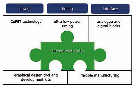
Fig 1: CMICs enable the creation of mixed signal circuits meeting the particular needs of the application
CMICs offer designers and manufacturers of wearable devices multiple advantages, including: optimised board space; a lower cost BoM; convenient innovation and prototyping; hard to copy designs; and a less complex and less stressful supply chain.
A dozen or more components can take up precious real estate in any system and today’s smartwatches and fitness bands can’t spare any board space, which could be better used for a larger battery or a slimmer form factor.
A CMIC can integrate several components into one product and, depending on the functions supported, these range in size from 8pin 1 x 1.2mm to 20pin 2 x 3mm STQFNs.
Board savings will depend on the type and number of functions implemented and customers have seen space reductions of up to 90% in devices which integrate up to 30 components, sometimes more.
Traditional circuit prototyping involves: circuit design; part selection; ordering samples and waiting for them to arrive; laying out a board; hand assembly; and debug.
This process can take days, if not weeks. Engineers don’t want to wait for parts to arrive or spend time doing tedious assembly. They want to get to work and get results quickly.
Prototyping with CMICs is faster and schematic capture, emulation and programming can be done in the same day. CMICs are similar to FPGAs but with analogue functionality. The CMIC process also makes ‘what if?’ exploration easier; changing a function is as easy as making the schematic change and programming a new part.

• The OTP NVM is cost efficient
• CMICs are designed and made in a single process node that is a ‘sweet spot’ for die size, analogue performance, digital density and cost per layer. They are assembled in a single packaging technology.
• Analogue components and discretes are priced relatively high on a per-function basis.
• The suppliers of analogue and discrete components are not motivated to reduce or improve their ASP product cost structure; for many, it would require going fabless or redesigning parts.
"It is easy to see how a CMIC allows for an easier design process and faster development. It is also easy to see how valuable board space can be saved." Mike Noonen
Confidential designs
A discrete circuit with off the shelf components is easy to copy or clone. A CMIC design is unique to the customer who designed it, making it difficult to copy or reverse engineer. This helps designers of consumer products to maintain a competitive advantage where there might be dozens of would-be competitors looking to ‘knock off’ their innovative designs. CMIC circuitry is as secure as a full custom IC and only the designer or their designated ODM and supply chain partners can procure it.
An important effect of avoiding or integrating multiple components is reduced supply chain complexity. Fewer parts to qualify, fewer to order and fewer to stock all have positive bottom line impacts. By reducing multiple parts, the risk of a component being in allocation or not being available is reduced – it only takes one discrete transistor to go on allocation or end of life to bring a line down or cause other serious issues.
CMICs offer many benefits that will make wearable designers’ work easier and their products more profitable. They are the ideal solution because board space is tight and needs to be maximised to save space for other valuable functions, such as a bigger battery. They also offer cost savings compared to traditional analogue and discrete devices, while reducing the risk and stress involved.
So, while wearable SoCs are not truly SoCs, the next best thing is a SoC with a CMIC.
Author profile:
Mike Noonen is vp of sales and business development with Silego.


