
Today's embedded products are far more complicated and sophisticated than those of just a few years ago. The design may include an FPGA along with a separate graphics processor (GPU), plus multiple connectivity ports for a video port, USB, Wi-Fi, and high-speed wired Ethernet, and perhaps the industrial ModBus or Fieldbus. Each of these processors and subsystems requires a unique clock frequency and type which is unrelated to the others, and therefore needs its own clock signal. Designing a system which generates these various clocks with the precision performance needed, and delivers them to their respective loads, are challenges which add to the other issues which the product engineers face.
The direct and obvious way to provide these clocks seems simple: use as many clock-generator ICs as needed, and place each next to its target load on the PC board, or use a clock tree driven by a master clock. Doing this solves the multiple-clock problem, at least in theory, as the needs of each load device are satisfied by a tailored clock signal which meets its unique requirements. Since each clock source is located close to its load, the crosstalk among clocks and between clocks and signals is reduced, thus minimising issues of added clock jitter and distortion.
This solution of using one clock IC for each target load seems attractive, but it has many negatives as well:
1.There's the immediate BOM (bill of materials) cost of the multiple, separate clock-generator ICs, and the logistics of managing and sourcing these different ICs.
2.A significant amount of PC board space is needed, which is a concern in almost every design.
3.If individual, single-output clock generators are used rather than a distributed clock tree, each needs its own crystal, adding to cost and board space;
4.Using a "clock tree" to generate the final clocks adds to cost, footprint, and clock jitter and error build-up
5.The use of multiple ICs increases overall power dissipation.
6.Using of multiple clock-generator ICs makes it more difficult to re-use of system designs across different products in a vendor's product line, since each new design may have a different layout and clock components.
How important each of these factors is in a given situation depends on the design, its priorities, and its tradeoffs. The decision to use one clock generator plus a crystal for each unique clock needed has many unintended consequences in multiprocessor systems.
An Alternative Approach Offers Advantages
Fortunately, there is another way which largely overcomes the drawbacks of using separate clock--generator ICs in multiprocessor designs. A multi-output, programmable clock generator can provide independent outputs from a single crystal and so can replace two, four, or more clocks. These ICs are available with a variety of output options, configurations, and frequency ranges, and target a range of applications.
When looking at a multi-output clock generator, it's critical to match its capabilities to the needs of the various clock loads. In many designs, the various loads not only have different frequencies, of course, but also different voltages, formats, rise/fall time maximum, and jitter specifications. The clock for a high-end FPGA or SoC device will have much tighter requirements than one for a low-speed communications link in the same design, yet the designer would like to choose a single clock-generator IC which can meet all the different needs.
The latest generation of these programmable clock generators can do this, especially for the difficult requirements. For example, the Xilinx Virtex-6 and Virtex-7 FPGAs include transceivers with data rates between 480Mbps and 6.6Gbps and between 2.488 and 11.18Gbps, a PCI Express Base with a raw data rate up to 5.0Gbps per lane, and an Ethernet MAC block supporting 10/100/1000Mbps links.
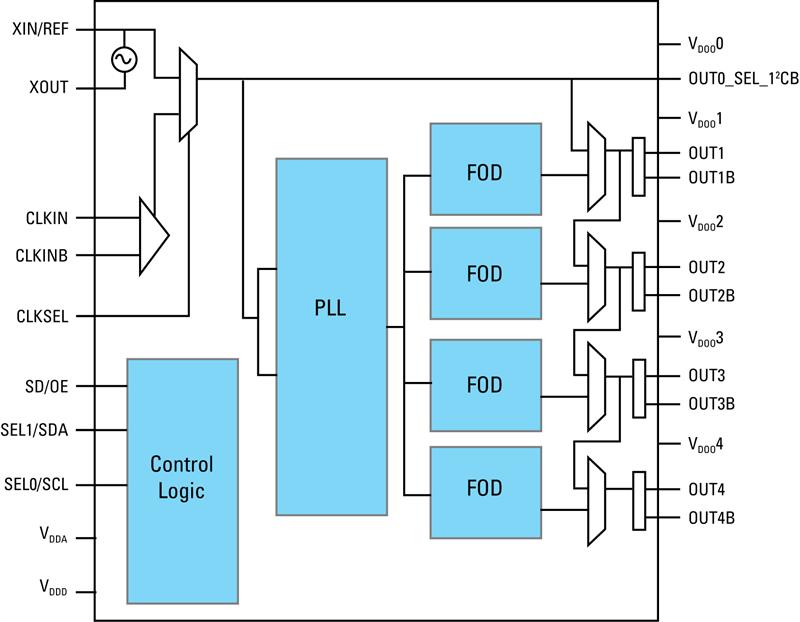
To meet the needs of designers implementing circuits based on these FPGAs, IDT introduced the VersaClock 6 series of programmable clock generators, Figure 1. The VersaClock 6 clock generators are available with between two and eight configurable outputs (selectable as LVDS or LVPECL); and two, three, or four one-time programmable (OTP) configurations, depending on specific device selected. All the clock generators incorporate a fractional-output divider architecture for maximum flexibility, and can produce any frequency between 1 and 350MHz. The most notable feature of the members of this family is their guaranteed RMS phase-jitter specification of well under 500fsec (0.5psec).
Application example illustrates the benefits
Designs which must support the SMPTE 424 standard are good examples of the benefits of using a programmable multi-output device. This standard, also known as 3G-SDI, has very stringent eye-jitter specifications for the high performance 3Gbps SerDes (serialiser/deserialiser) function in order to meet the desired bit error rate (BER) goals. [SMPTE – the Society of Motion Picture & Television Engineering – is an internationally recognized standards body whose governing specifications include the high-speed serial physical interfaces for transmission of digital TV, commonly called SDI or Serial Data Interface.] The key mandates are:
• Timing jitter specification of 2.0 UI maximum, peak to peak, from 10Hz to 100kHz
• Alignment jitter specification of 0.3 UI maximum, peak to peak, from 100kHz to 297MHz); with 0.2 UI recommended
(A unit interval (UI) is the time between two adjacent signal transitions, and the reciprocal of clock frequency.)
To further add to the technical challenge, many broadcast video designs need to support both NTSC and PAL HDTV standards, which means they need to simultaneously have both 148.5MHz and 148.5/(1.001)MHz reference clocks. In addition, the trend of broadcast video products supporting Video-Over-IP (VoIP) means the design may also need to support 10GE PHYs (10gigabit Ethernet Physical Layer), so an additional reference clock at 156.25MHz is typically required.
Due to their integrated, high-performance GTX/GTH/GTP transceivers, the Xilinx 7 Series FPGAs are often chosen for these SMPTE-compliant designs. To meet the SMPTE 424 eye-jitter specifications, Xilinx specifies very tight dBc/Hz phase-noise requirements for the reference clock used to drive these SerDes functions. If the same Xilinx 7 Series GTX/GTH/GTP transceivers are also used to implement the 10Gbps SerDes, the very tight dBc/Hz phase noise requirements are again critical. These non-integer-related clock frequencies (148.5 MHz, 148.351648 MHz, 156.25MHz), when combined with very tight phase-noise requirements for each clock, mean that providing an integrated clock solution is a major task.
Fortunately, there is a single device which can synthesise all of these high-performance clocks in a single device: IDT’s Universal Frequency Translator (UFT) family of high-end PLLs. This family can be used as a high-performance synthesizer, requiring only a simple, fundamental-mode parallel-resonant crystal for its input reference. Members of the UFT family support either one or two different pin-selectable configurations per PLL, and these may be pre-loaded into the internal one-time programmable (OTP) non-volatile memory for automatic operation directly from power up, or an I2C serial interface can be used to set the desired frequency translation configurations.
For the SMPTE 424 design, IDT's 8T49N241 can be used as a high-performance, four-output synthesizer, in which the savings in board real estate and design complexity are clear. Clock devices in this family have the performance required for Xilinx 7 Series reference-clock in this difficult application.
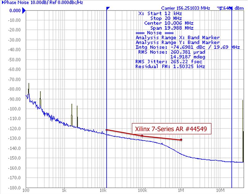
Figure 2 shows a typical phase-noise plot for a 156.25MHz output clock generated by an IDT UFT clock device. The phase-noise plot is well below the phase-noise mask defined in Xilinx Action Note AR# 44549.
If a designer chooses to use a single clock generator IC with multiple outputs, many of the issues which are due to use of separate clock ICs disappear or become much simpler. Further, by adding programmability to the clock IC, the same component and layout can be used across multiple or upgraded products.
There is one point that the designer must keep in mind when using a single clock IC. The physical placement of this IC, along with the PC-board routing of its various outputs to their respective loads, must be modelled and simulated. This is needed to maintain clock-signal integrity and keep crosstalk and noise, as well affect on jitter, to a low-enough level. Fortunately, the simulation tools now available for high-speed signals and layouts make this possible, and will also help ensure overall design performance for non-clock signals as well,
Tools, ease of use are also design considerations
Obviously, a user-programmable, fully configurable IC such as a clock generator is frustrating to users if it can’t be easily programmed or configured. IDT's Timing Commander software platform lets customers to configure and program devices with an intuitive and flexible graphical user interface (GUI).
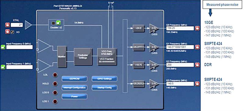
A screen capture of the platform's GUI when used to configure the 8T49N241 as a high-performance four-output synthesizer in the SMPTE 424 applications demonstrates this, Figure 3. The combination of a fractional-feedback PLL and a mix of integer and fractional output dividers allow the 8T49N241 to generate all of these output frequencies with 0ppb (parts per billion) additive synthesis error, and the measured phase-noise performance of the 10GE and SMPTE 424 clocks meets the Xilinx 7 Series requirements.
Further, the in-system I2C programming mode can be used to program the some of the multi-output devices at power-up, to override the one-time programmable (OTP) memory configuration and so reconfigure the device, if required. Finally, users can additionally program an independent spread-spectrum capability on each output pair, to attenuate system-level EMI/RFI levels and associated concerns, again depending on device selected.
User programmability serves the designer of multiprocessor systems in many ways and overcomes many of the drawbacks of using individual, independent clock-generators, and does so without sacrificing performance. The programmability supports different types and needs of loads with a single device, so issues related to "which clock for which load type?" are resolved. They allow tailoring of frequency, of course, but also other critical specifications which make the difference between a cost-, performance-, and power-efficient design compared to one with too many compromises.
Author profile
Baljit Chandhoke, product line manager, Integrated Device Technology


