
Challenging applications require ever smaller components to fit into wearable devices or reduce size and weight in mobile applications, but also increasingly in other consumer devices, along with industrial, medical and automotive applications.
While the path to miniaturisation in purely digital applications is well-trodden, in analogue and power the approach remains possible, yet far less obvious.
In this article we take a look at the challenges in reducing mixed-signal devices and discuss some of the approaches that can be used.
There is a long-held expectation that every generation of technology will be smaller or more powerful than its predecessor – or both. There are many reasons for this – reducing weight in electric vehicles to increase their range, reducing the size of industrial equipment such as robots, and making our personal devices more appealing and convenient.
The challenge with analogue and power
Stretching back to the 1960s when ‘Moores Law’ was first coined, the basic integrated circuit technology that underpins electronic designs was expected to show significant growth in complexity matched with size and cost reductions every couple of years. This has largely held true, especially in the world of pure digital devices such as logic ICs and MCUs. Here, size reduction is primarily concerned with reducing feature sizes through process evolution and is largely driven by electronic design automation (EDA).
However, in the world of analogue and power, things are somewhat different. Here the approach to size reduction concentrates more on the ability to combine design blocks and improving the design to allow this to happen.
Some components, such as power MOSFETs, require a certain physical size to be able to deliver low ohmic (static) losses and handle the higher currents that modern applications often require.
Unless the design can be improved to reduce power consumption, the laws of physics define the size of these types of components.
Key to integrating analogue and power designs, along with digital logic is the ability to merge different manufacturing processes – a common base is required to achieve the highest levels of integration.
Thinking differently
To the casual observer, miniaturisation is simply squeezing the size of the semiconductor package into a smaller size and while this can deliver some benefits, there is often a better approach.
Ultimately, the system designer is seeking a reduction in size and weight of the end design and requires semiconductor devices that allow this to be achieved depending on the entire circumstances of the project.
Often termed ‘meaningful shrinkage’ this reflects the fact that a change in a semiconductor device may allow size reductions elsewhere that are many times larger than the semiconductor itself.
An example of this is the move of MOSFET devices from silicon (Si) to wide-bandgap (WBG) materials such as silicon carbide (SiC) or gallium nitride (GaN) materials.
Through a reduction in gate charge (Qg) these devices are able to operate more efficiently at high frequencies. As a consequence of the frequency, the size of magnetic devices is reduced as is the size of thermal management (such as heatsinking) due to the enhanced efficiency. Other examples of revised semiconductor designs driving design benefits include advanced motor controllers that are able to operate without the need for external components, such as shunt resistors.
Areas for consideration
Along with the connectivity between the various building blocks within a mixed signal semiconductor, there are a myriad of other considerations that must be taken into account. Inevitably, this requires a significant amount of trading off and, for this reason, requires highly experienced designers.
The process starts with a thorough understanding of the application(s) that the device will be used in. From there, the interfaces between each of the blocks are considered to ensure that drive strength (energy supplied from one block to another) is adequate but not over-specified.
In some cases, there may be a benefit in moving some functions from the analogue domain to digital, but in some cases, this may not suit the application, driven by aspects of accuracy, reliability, and performance.
One of the primary considerations is the path for conductivity losses, both electrical and thermal.
Heat generation is one factor which drives size in semiconductors, so it is important to minimise losses.
As an example, designers must consider the trade-offs between wire bonds or a copper clip for connecting the die to the package – not only from an electrical and thermal perspective, but also with regard to manufacturability, yield and reliability. Minimising the thermal conductivity losses may require advanced packaging that offers double-sided cooling although there can be cost implications associated with this.
In challenging applications/environments, such as those found in under-the-hood automotive applications, careful consideration must be given to materials. With the extreme (and rapid) swings in temperature, the substrate and other components may expand and contract at different rates (differential coefficient of thermal expansion – CTH), which will put stress on joints, leading to reliability issues. Materials such as substrates and glues must be carefully chosen to suit the environment of the application.
In almost all cases ‘manageable’ is a better goal than ‘smaller’ – for example the automotive industry has a particular need for automated optical inspection (AOI) that requires visible leads that, ultimately, defines how small a package can be.
Design example – motor controller
Motor controllers are relatively complex devices and, therefore, serve as a good example of the process of integration and miniaturisation. Typically, these devices consist of control logic, gate drivers and MOSFETs that can be integrated in various combinations. Aside from what may be physically possible, the priority for the designer is to determine what is meaningful to integrate.
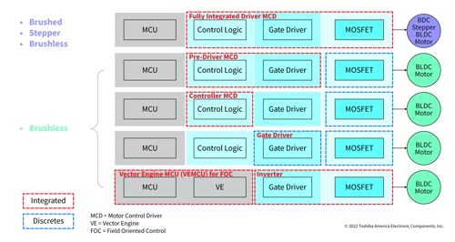
Figure 1: Multiple integration approaches are possible for MCDs
Clearly, a fully integrated solution could contain all of the major building blocks. However, while this is attractive from the perspective of neatness, it limits the flexibility. An alternative approach integrates just the control logic and gate drivers, leaving the MOSFETs as discrete external devices. This allows the MOSFETs to be sized for a number of different applications, giving a wider appeal (and a higher manufacturing volume which will be beneficial to cost).
The incorporation of novel design techniques within the control logic can benefit the design and ease the process of integration and miniaturisation. For example, intelligent phase control brings the current and voltage into the same phase, thereby reducing the power factor and the energy consumed – increasing efficiency as well as reducing the operating costs of the motor.
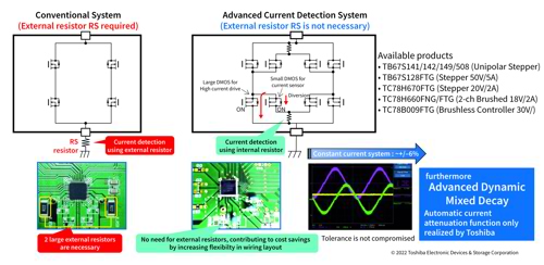
Figure 2: Innovative design techniques support the integration / miniaturisation process
In a conventional motor drive system, a pair of (fairly large) external current sense resistors are required. However, the Advanced Current Detection System (ACDS) developed by Toshiba replaces the external resistors with an intelligent and very precise integrated measurement circuit, simplifying the PCB layout and saving space in the final design.
Other techniques can be incorporated, such as the Advanced Dynamic Mixed Decay (ADMD) that tracks input current very precisely, allowing highly efficient motor control possible at high RPM.
In addition, sensorless motor control techniques remove the need for external Hall Effect sensors, further reducing size, BOM cost and complexity.
Commercial considerations
While many approaches may be technically possible, there is an overriding requirement to be mindful of commercial considerations when integrating and reducing integrated circuits.
Sourcing professionals are increasingly driven by multi-source policies that require footprint compatible devices to be available from multiple manufacturers.
While this is a significant topic, in its own right, it is leading many semiconductor companies to retain industry standard footprints and pin assignments for their devices.
Even with this requirement, there is still the opportunity to differentiate through good design and innovative techniques, such as those outlined above.
Summary
Miniaturisation of mixed signal integrated circuits that contain analogue and / or power elements is very different to shrinking a digital IC. Due to mixed processes a different approach is needed and, often, the size of the IC may not reduce, but significant size benefits may be derived elsewhere in the end product.
When it comes to managing the complex trade-offs and decisions about what to integrate (and how) as well as the commercial considerations, highly experienced engineers are a must for any successful project.
Author details: Armin Derpmanns, General Manager Semiconductor Marketing, Toshiba Electronics Europe


