
Hot swap controller ICs enable such board insertion and removal from live systems by soft starting the supply, avoiding connection sparks, backplane supply glitches and card resets. The controller IC drives a power MOSFET switch placed in series with the supply entering the board (see figure 1). After the board is plugged in, the MOSFET switch is turned on slowly such that the inrush current which charges the load capacitors is kept at a safe level.
When hot swap circuits fail, the Achilles’ heel is often the MOSFET switch, which in turn may damage or destroy the hot swap controller. The common reason for MOSFET failure is that insufficient attention was paid to its safe operating area (SOA) during selection. Instead, the MOSFET may have been selected primarily for its drain-source on resistance (Rds(on)) and maximum drain current (Id(max)). The new design may also have been based on an older one with lower load capacitance in which the same MOSFET worked perfectly.
Since the majority of power MOSFETs are optimised for low Rds(on) and fast switching – and most power system designers are habituated to selecting MOSFETs for those characteristics – SOA gets overlooked in circuits where the MOSFET spends significant time transitioning through the high-dissipation switching state. It does not help that SOA is not featured in MOSFET manufacturers’ parametric selection tables. Even when attention is paid to SOA, the amount of derating or margin to apply is not evident as the SOA data is often based on calculations instead of test data.
Safe operating area
The SOA is a measure of a MOSFET’s power handling capacity for pulsed and DC loads and is usually illustrated by a graph in the MOSFET datasheet. The x-axis is usually the MOSFET drain-to-source voltage (Vds), while the y-axis is usally drain current (Id), with both axes plotted using a logarithmic scale. On such graphs, straight lines (each for different pulse width, tp) depict constant MOSFET power and each line represents the power dissipation allowed in the MOSFET for a specific tp – and tp can range from microseconds to infinity (DC). For instance, for a 10ms wide pulse, a MOSFET could support 5V from drain to source with 50A flowing through it. This equates to a power dissipation of 250W. Lower power for the same pulse width ensures safe MOSFET operation, which would be denoted as an area of the graph beneath the 10ms line – and this leads to the term safe operating area. The extremities of the graph are determined by on-resistance, drain-source breakdown voltage and maximum pulsed drain current.
Why is SOA important?
Most power MOSFETs are applied in circuits where they switch on and off quickly, spending only nanoseconds in the high dissipation transition state. In such applications, SOA is not a primary concern. In contrast, SOA is very important in hot swap circuits, which provide inrush current control (soft start), current limiting and circuit breaker functions. To understand why, let’s think about start-up waveforms for a hot-pluggable board. When the board is inserted into a 12V backplane supply, the hot swap controller waits for the connector contact bounce to finish before soft-starting the MOSFET gate. The output voltage follows and reaches 12V in 40ms. For this soft-start period, a capacitive charge current of 200mA will flow through the MOSFET while Vds ramps down from 12V (12Vin − 0Vout) to almost 0V 12Vin − 12Vout). When a short-circuit occurs at the load, the controller will limit the current to 6A with 12V ( 12Vin − 0Vout) across the MOSFET. This 72W dissipation state lasts for 1.2ms until the circuit breaker timer expires. In situations such as start-up inrush and current limiting, a hot swap MOSFET is required to handle significant power for periods ranging from hundreds of microseconds to tens of milliseconds and attention needs to be paid to its SOA performance.
Guaranteed SOA
Linear Technology offers a family of integrated MOSFET hot swap controllers that simplifies the hot swap designer’s task by eliminating the time spent scouring MOSFET data sheets for the best fit.
The latest additions to the family – the LTC4233 and LTC4234 (see fig 2) – are 10A and 20A hot swap controllers respectively, with integrated MOSFET and current sensing for supplies ranging from 2.9V to 15V. Thiscovers the standard supplies of 3.3V, 5V and 12V. By integrating the two most critical and largest hot swap components – the power MOSFET and sense resistor – these controllers free design time better spent on adding more valuable features to the end product and also release board area.
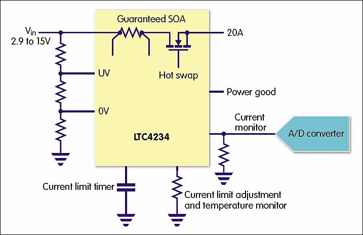
Figure 2: The LTC4234 is a 20A hot swap controllor with a guaranteed safe operating area
A feature of the LTC4233 and LTC4234 controllers that is not found in standalone MOSFETs is that the internal MOSFET’s SOA is guaranteed in the data sheet and each device’s SOA is production tested at a single point on the SOA graph. Figure 3 shows the SOA graph for the LTC4234. Its SOA is tested by applying 13.5V from input to output and sourcing 6A from the output for 30ms. The resulting power dissipation is 81W – shown by the red dot in the graph. The LTC4233 is tested with the same voltage, but with 3A, equating to 40.5W for the same time period. Bear in mind that the SOA graphs for the LTC4233 and LTC4234 show the minimum guaranteed SOA, whereas MOSFET data sheets show typical values.
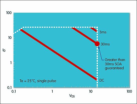
Figure 3: The guaranteed safe operating area graph for the LTC4234
The LTC4233 and LTC4234 also output a ground-referenced signal proportional to the load current passing through the internal sense resistor. This output can be measured with an external A/D converter (see figure 2) to provide board current and power consumption data to the system manager. The current limit is reduced from its default value with a single external resistor, affording quick adjustment for dynamic load changes and various applications. Selectable undervoltage and overvoltage thresholds protect downstream loads against voltages outside a valid window, preventing circuit malfunction and damage. Even where hot-plug is not required, the controllers perform inrush current control, current limiting and circuit breaker functions.
Typical applications for these controllers are on space-constrained high-density boards and cards in mission critical servers, network routers and switches, enterprise solid state storage and industrial systems.
Conclusion
Hot swap circuits are the gateway to board power and a MOSFET failure can damage the expensive processing electronics downstream of the device, in addition to the hot swap controller itself. Field failures, exposing MOSFET weakness, may involve costly recalls and consequent damage to reputation. Therefore, it is important to ensure that the chosen MOSFET reliably handles the stresses encountered in hot plug applications. The LTC4233 and LTC4234 integrated MOSFET hot swap controllers shrink solution footprint and design time while also guaranteeing a rugged and reliable solution with their novel production testing of every controller’s SOA.
Author profile
Pinkesh Sachdev is a senior product marketing engineer for mixed signal products with Linear Technology.


