
To further improve reliability, multiple power supply modules are combined in parallel to guarantee continued operation through any single supply failure. Supplies can be paralleled using power Schottky diodes in a diode-OR configuration. Some systems OR identical supplies while others OR a backup battery, an auxiliary maintenance supply, or a capacitor bank. In the latter case, the backup supply is only needed when the main supply is absent. Also, diodes in combination with hold-up capacitors on the output side are employed to provide ride-through during power supply brownouts.
At current levels above a few Amps, Schottky diodes dissipate a lot of power, around 0.5W for every 1A flowing through them, and they drop voltage, a precious resource for lower voltage 3.3V and 5V supplies. An ideal diode, built out of a low-resistance MOSFET switch and a controller, lowers the power dissipation and voltage drop by a factor of ten or more, eliminating heat sinks and conserving board area. Ideal diode controllers have been integrated with Hot Swap controllers in several configurations to provide compact solutions for the various hot plug and ORing scenarios encountered in high availability systems.
Some high availability systems combine multiple power modules on the backplane and bus the supply output to all the load cards in the system (Figure 1a). When power modules plug into a live supply bus, both Hot Swap (denoted by switch in figure) and diode control are required. For the first module insertion, the Hot Swap controller soft-starts the supply bus, gently bringing up the bulk capacitors at safe current levels. For a second module insertion in to a powered bus, the ideal diode control ensures that there is no back-feeding if the module voltage is lower than the bus voltage. On the other hand, the Hot Swap control ensures safe inrush levels if the second module voltage is higher than that of the bus. The Hot Swap controller also provides a fast-acting current limit that is in addition to the power supply’s own current limit. Each load card implements hot plug capability as they share a common supply bus.
The LTC4229 is a 2.9 to 18V single supply ideal diode and Hot Swap controller (Figure 1b) that can be employed on a plug-in supply module shown in Figure 1a. Its 2.9 to 18V operating range accommodates 3.3V, 5V, and 12V supplies. It controls all N-channel MOSFETs to reduce voltage and power loss from input to output. Unlike passive diodes and fuses, the LTC4229 provides multiple power status outputs.
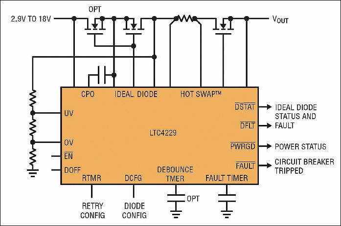
Figure 1b: LTC4229: Single ideal diode and hot swap controller for power supply ORing and holdup applications
Load Card
The Figure 1a topology minimises cost as the load cards only need to implement Hot Swap control. The downside of this configuration is that the diodes on the backplane have to be large to support the entire system current and are therefore more prone to failure. A diode failure disables that power supply path for the entire system and this may not even be noticed until the other supply fails, leading to
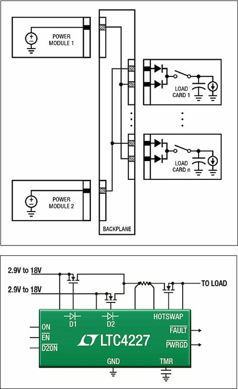
The LTC4227 from Linear is a dual ideal diode-OR followed by a single Hot Swap controller (Figure 2b), providing a compact solution for load card supply ORing and hot plug. The ideal diode-OR (D1 and D2) powers the card with the highest voltage supply while the Hot Swap controller manages inrush current and provides short-circuit protection with a current-limited circuit breaker.
The Figure 2a topology adds cost to each load card by requiring supply ORing on it. Since a system typically has more load cards than power modules, it is beneficial to make the load cards simpler. The topology of Figure 3 achieves both high reliability and simpler load cards by employing power modules with an independent output for each load card. Each output path has a diode and inrush control switch. The outputs are combined on the backplane for each load card. The load cards are simplified at the expense of increased cost and complexity in the power modules.
For the Figure 4a topology, the LTC4228 is a dual ideal diode and Hot Swap controller (Figure 4b) for 2.9 to 18V supply modules with multiple outputs, such as multiple 12V in a µTCA system or a 12V and 3.3V in a PCI Express system.
Figure 2a (right, above): Power supplies ORed on the load card. Figure 2b (right, below): LTC4227: Dual ideal diode-OR and single hot swap controller for supply ORing application on a load card
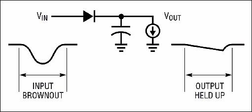
Figure 3: Power supply holdup with inline diode and output capacitors
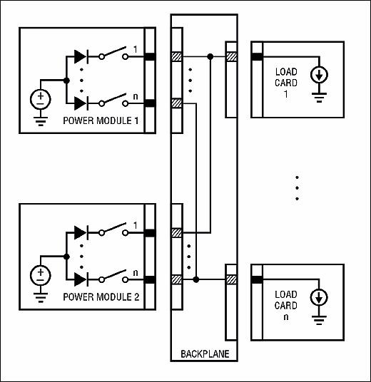 | 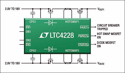 |
Figure 4a (above, left): Power modules with independent ORed outputs for each load card. Figure 4b (above, right): LTC4228: Dual ideal diode and hot swap controller for multiple power supply ORing and holdup applications.
Supply holdup
Some power sources experience brief brownouts lasting from a few hundred microseconds to many milliseconds. On a shared backplane supply, this may occur as load cards turn on or as the supply bus switches between ORed supplies. To provide ride-through for the load cards, an ideal diode is inserted in the supply path at the input to the card (Figure 3). When the input supply dips, the diode opens the supply path, blocking any current flow back towards the backplane. The card continues to power itself from bulk capacitors at the output side of the diode until the input supply recovers.
The LTC4229 holds up a supply when positioned at the power entry to the card. To prevent the Hot Swap controller from turning off due to an under-voltage condition, the ideal diode is positioned in front of the Hot Swap controller as shown in Figure 1b. If needed, the LTC4229 allows the Hot Swap controller to be positioned before the ideal diode controller. It is flexible enough that the Hot Swap and ideal diode control can each be used independently on separate supplies. The LTC4228 provides holdup for two separate power supplies.
Supply prioritisation
When the ORed supplies are disparate types, one of them is usually a backup supply - a battery, low current auxiliary supply, or capacitor bank - meant to provide power when the main supply is absent. The main supply is assigned higher priority than the backup supply, but is not necessarily the higher voltage of the two and therefore simple diodes cannot be used to combine them.
This is a prioritiser application: power sources are selected by priority, not on the basis of voltage.
When the backup voltage is higher than the main voltage, the backup supply needs to be blocked from powering the output as long as the main supply is present. This is shown in Figure 5 with the LTC4229 and the LTC4352 ideal diode controller. Back-to-back MOSFETs (MD1 as switch and MD2 as ideal diode) are controlled by the LTC4229 to block the 12V battery from powering the output as long as the primary voltage is above 4.7V (set by R6-R7-R8 divider). When the primary supply drops below 4.7V, the LTC4229 turns MD1 and MD2 on and power is supplied from the 12V backup battery.
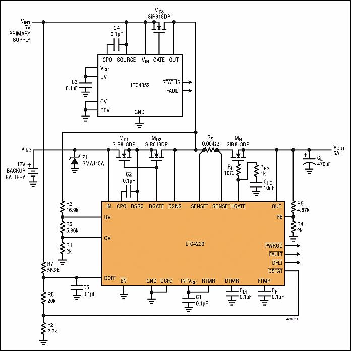
Figure 5. Prioritiser application with 5V main supply (1st priority) and 12V backup battery (2nd priority)
Conclusion
High availability systems need both hot plug and diode control to combine multiple power supplies for redundancy and reliability. The LTC4227, LTC4228, and LTC4229 provide different configurations suited for the various locations where supply ORing or holdup is required: on the power supply side or on the load card side. These controllers are combined with other stand-alone ideal diode and Hot Swap controllers to address supply prioritisation and other custom applications.
Author details
Pinkesh Sachdev is a product marketing engineer, Mixed Signal Products, Linear Technology.


