
A derivative of the company’s DragonBall range, the first i.MX parts – a contraction for Innovative Multimedia eXtension – found application in consumer products such as e-readers, building on DragonBall’s success in products such as the Palm computer.
Freescale is now part of NXP and Ron Martino is the company’s vp with responsibility for the i.MX product lines. “Freescale had built a strong position in the consumer market with i.MX, then moved into automotive infotainment. In consumer, the device was seen to be power efficient, with a hardware accelerator for electrophorescent displays, while automotive developers saw a scalable platform with pin compatibility. This gave the ability to adapt the end system, cut time to market and get better development efficiency.”
Since then, the portfolio has expanded to eight families, with the latest devices featuring advanced ARM cores and manufactured on leading edge processes.
“Since 2011,” Martino contended, “there has been explosive growth in demand, with shipments growing at 20% per year. And we haven’t cancelled a single i.MX device since we launched the programme.
We’re a trusted supplier,” he continued, “supporting industrial parts for 10 years and automotive parts for 15 years.”
While DragonBalls were based on Motorola cores, i.MX parts are ARM based. Martino noted: “For example, the i.MX2 featured the ARM926 core, but the range has evolved to use Cortex-A8, A9, A35 and A53 cores, so we are now offering the benefits of ARM’s 64bit v8 architecture.”
And the i.MX2 is still seeing design wins. Martino ascribed this to the device being optimised for an efficient Bill of Materials (BoM) and featuring integrated power management.
Until the i.MX6 was launched, only single core devices were offered. That introduction added single Cortex-A7 parts, as well as single, dual and quad Cortex-A9 variants. Since then, shipments have boomed. “The i.MX6 range has four times the volume of previous devices,” Martino noted. “NXP now has the widest range of application processors and we continue to spin variants of the i.MX6.”
Within the i.MX6 range, the i.MX6SoloX represented something of a watershed, adding a Cortex-M4 core for real time operations. “It’s a single part, but with two domains,” Martino explained. “From then on, all i.MX parts have real time domains, plus different optimisations. In general, the range is suitable for all embedded processing applications, ranging from e-readers and smart thermostats to point of sale systems and building controls. And automotive designers are focusing on clusters and V2X applications.”
Process technology has also brought significant benefits. While the i.MX6 range is manufactured on a 40nm low power process, the succeeding generations have moved to 28nm – and the recently announced i.MX7ULP is set to be made using FD-SOI technology. “As we go from 40LP to 28 FDSOI,” Martino explained, “we have a broader dynamic range in terms of power and performance. In particular, we can cut dynamic power and stand by power dramatically compared with the i.MX6.”
Martino noted that the i.MX7Solo and Dual, made using a 28nm bulk CMOS process, cut power consumption by a third compared to the i.MX6 series, FD-SOI allows further savings. “We have reduced power consumption in the i.MX7ULP to about 30µA/MHz. While that’s world class, we have developments in process that show we can reduce that figure to less than 10µA/MHz in certain implementations. That will make it very power efficient for battery operated devices.”
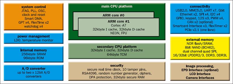
Simplified block diagram of the i.MX7Dual processor
The FD-SOI process allows NXP to ‘tune’ devices for particular applications. “We can use reverse body biasing to optimise parts for the most efficient frequency and power consumption, but we can also use forward biasing to push performance at the high end and get a significant increase.”
The i.MX7 range also sees a slight change in focus. “There are a couple of modifications in our approach,” Martino noted. “One of these is a branch to focus on battery operated devices. There’s also a branch featuring more independent control and power domains, building on the Cortex-A7 and Cortex-M4 cores. These developments enable something we see as being important for battery powered devices; the ability to bring systems up in different ways.”
But why should an embedded system developer think about designing around an i.MX7ULP, for example, rather than a ‘traditional’ MCU? Martino: “One reason is that it simplifies the BoM. With the 7ULP, designers will have access to a flashless MCU, plus an applications class processor core on the same piece of silicon. It will give them the flexibility to work between the two domains. Not only that, standby power consumption is only 15µW and the part offers very efficient graphics.”
Launched alongside the 7ULP at Embedded World, the i.MX8X family is aimed at industrial automation, industrial control and robotics applications, as well as at the automotive sector.
The family offers parts with up to four Cortex-A35 cores and a Cortex-M4F core, along with hardware accelerated graphics and video engines. Capable of driving up to three displays simultaneously, the i.MX8X series offers power and performance. “We’re pushing a Cortex-A35 core to 1.26GHz,” Martino continued, “and we can optimise power and cost as key variables. Not only can users scale system performance, they also have software reuse. The i.MX8X range is an evolution of the i.MX6, bringing more performance at roughly the same cost. But it also brings features such as vision detection and hardware virtualisation.”

Will specifying an i.MX7 or 8 bring issues for embedded system developers? Martino, pictured right, said: “There will be some applications where companies might want to run an RTOS in the Cortex-A and -M domains. But when you’re dealing with graphics, Linux and Android, you’re going to need different IDEs and complexity will be greater, especially as you will be dealing with DDR interfaces.
“However, for real time applications, the development flow will be pretty much traditional, with the exception of when the Cortex-M4 will be used to offload work from the other domain. Then, designers will need to determine how the workloads are handled.”
One particular application which might be suited to the i.MX7ULP – or a future variant – is IoT edge node devices. Geoff Lees, general manager of NXP’s MCU business, pointed towards this a couple of years ago, when he told New Electronics: “We are beginning to see more IoT applications suited to low end Cortex-A processors, rather than high end Cortex-M cores.”
Martino commented: “We could take the 7ULP and pull out the real time domain, creating a Cortex-A based chip optimised for much lower performance, but which can still handle an RTOS or a rich OS. And the real time capability of devices we will be introducing should fit IoT applications nicely, giving developers flexibility, along with low cost and power consumption.”
Perhaps there’s a glimpse at a future direction for the i.MX road map when Martino concluded: “With FD-SOI, we see the ability to integrate novel non volatile memory, as well as RF functionality.”


