
Typically undertaken in a laboratory, this process relies heavily on automated procedures to verify and then return results to the end user. Laboratories use advanced informatics systems that link multiple computer terminals with different end users, central servers, physical autoanalyser instruments, and other devices – making the process both costly and complex.
Nanomedical Diagnostics has come up with a Field Effect Biosensing (FEB) technology that provides real-time, label-free kinetic binding and affinity data.
“It’s a novel sensing technique that will be available to more pharmaceutical companies seeking to characterise biomolecules quickly and easily. We think it could radically transform the field of drug discovery,” suggests Mitch Lerner, vice president of production at Nanomedical Diagnostics.
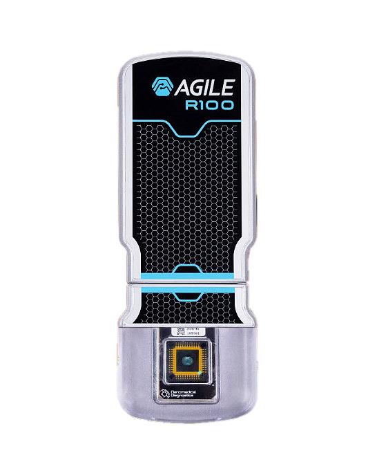
“This is the only mass-produced graphene biosensor currently available on the market,” explains Lerner. “The benefits of graphene technology have traditionally been restricted to specialised, well-funded university laboratories looking to build one-off platforms. Our new sensor device, the AGILE-100, makes this new sensing technique available to any pharmaceutical company looking to characterise biomolecules.”
The device is intended to provide pharmaceutical and biotherapeutics companies with more informed decisions earlier in the drug discovery process and that data can be processed by using either a regular laptop or smartphone.
“We want to transform the field of drug discovery,” says Angela Shue, vice president of marketing. “Traditional methods of drug development rely on extensive screening and high throughput, which is expensive and lacks kinetic data.
“The graphene biosensor technology will drastically lower the cost of entry and provide more portability and throughput than other technologies. Going forward, we see this playing not only in life science research and diagnostics, but also in portable – or even implantable – health monitoring devices,” Shue suggests.
Manufacturing process
According to Lerner and Shue, the most difficult part of bringing the product to market proved to be developing a cost effective large scale manufacturing process.

“Which is where Rogue Valley Microdevices (RVM) came in,” explains Lerner, pictured left.
When it launched the graphene biosensors earlier this year Nanomedical Diagnostics described Rogue Valley Microdevices as, “key to developing a viable large-scale fabrication process to produce these biosensor chips.”
Nanomedical Diagnostics CEO, Ross Bundy, said “RVM’s engineers came up with a process that enabled the AGILE to be manufactured with high reproducibility, quality, and throughput, providing better data and lower costs.”
Graphene has long been touted as possibly the world’s most versatile material since its discovery in 2004, capable of revolutionising a range of different fields.
“Graphene is great for biomedical applications because it provides excellent electrical conductivity, a high surface area, and carbon based unique biocompatibility,” explains Lerner.
“What we needed was a material of the highest quality that provided the highest mobility at the lowest resistance. We are looking at events at the nanometre level and need to interface with active proteins that cannot be permitted to get contaminated. If they lose their biological functionality, then the sensor is unable to work.”
Comprising of a two dimensionally hexagonally arranged set of carbon atoms, graphene offers the highest room temperature mobility of any material and, as such, is attractive for semiconductor devices. Being two dimensional, every graphene atom is in direct contact with its environment, making it perfect for use in sensing applications.
Studies on the detection of biomolecules using lab-produced graphene-based biosensors have shown that graphene sensors exhibit high sensitivities, wide linear detection ranges, and low detection limits.
So, what has been holding back the use of graphene?
Numerous efforts have been made to commercialise graphene biosensors at scale, but the process has been hampered because of the difficulty of integrating delicate graphene material into standard high-volume production processes.
From producing quality graphene in large quantities to removing graphene from its growth substrate and moving it to its target substrate, as well as integrating graphene with conventional electronic measurement systems, the challenges to using graphene at scale are formidable.
“When Nanomedical Diagnostics approached us, we recognised the opportunity to get in on the ground floor of a revolution,” says Jessica Gomez, founder and CEO of Rogue Valley Microdevices, a full-service precision MEMS foundry that specialises in MEMS and biomedical device manufacturing.
“As a company we take customers from the early R&D stage, through pilot, then into full production,” she explains, “but working with Nanomedical Diagnostics was a challenge. There’s not a lot of information out there when it comes to working with graphene mid-process, or how other materials will work with graphene post deposition. Crucially, we needed to develop a manufacturing methodology that was robust.”
In MEMS, materials are used for both their electrical and mechanical properties, so RVM also had to take into consideration the preparation of surfaces and the potential problems associated with using graphene.
Right: Nanomedical Diagnostic's AGILE-100 is the first mass produced graphene biosensor currently available on the market.
“We needed to create a cost structure that made sense,” Gomez says.
“While academic groups know how to do some graphene processing steps, their goal is not yield,” explains Lerner. “They need to make a couple devices to get a paper published and move on. We need every transistor to work because every broken transistor eats into our bottom line. Even worse, any failed transistor that gets through to a customer hurts the quality of our product and our reputation.”
When it comes to producing a graphene biosensor there are a number of process steps that need to be taken into account, including electrode patterning, graphene growth and deposition, graphene patterning, and finally wafer passivation with a dielectric.

“The graphene we grow is more crystallographically pure than any we could find on the market as verified by Raman and electronic transport measurements,” explains Lerner. “Our graphene deposition technique results in less contamination and hence less doping than any other technique.”
“What RVM was able to do was figure out how to take that wafer through lithography, etch, and oxide deposition without introducing any significant contamination, a process that again was verified,” explains Gomez, pictured left.
According to both Gomez and Lerner, RVM could bring to bear a number of tricks: optimising the type of resist to reduce graphene contamination; making the resist of the strippers more compatible with graphene’s chemistry; the optimisation for oxide adhesion to the graphene; and etching expertise to avoid over-etching or under-etching, both of which would have made the sensor nonviable.
“Ultimately the greatest proof that this process has worked,” says Lerner “is that we are actually selling a tool and people are buying it. While there may be other graphene sensor companies out there, none of them, at present, have a tool that is currently available on the market.
“We’ve got repeat customers for our graphene sensors and have been able to publish results in leading scientific journals like Nature and JACS. And that performance comes directly from the reproducibility and yield and quality afforded by the joint actions of Rogue Valley Microdevices and Nanomedical Diagnostics.”


