
The lock-in amplifier makes the physical quantity to be measured periodic by shifting the DC signal to a known frequency and thus avoiding a high level of low-frequency flicker noise.
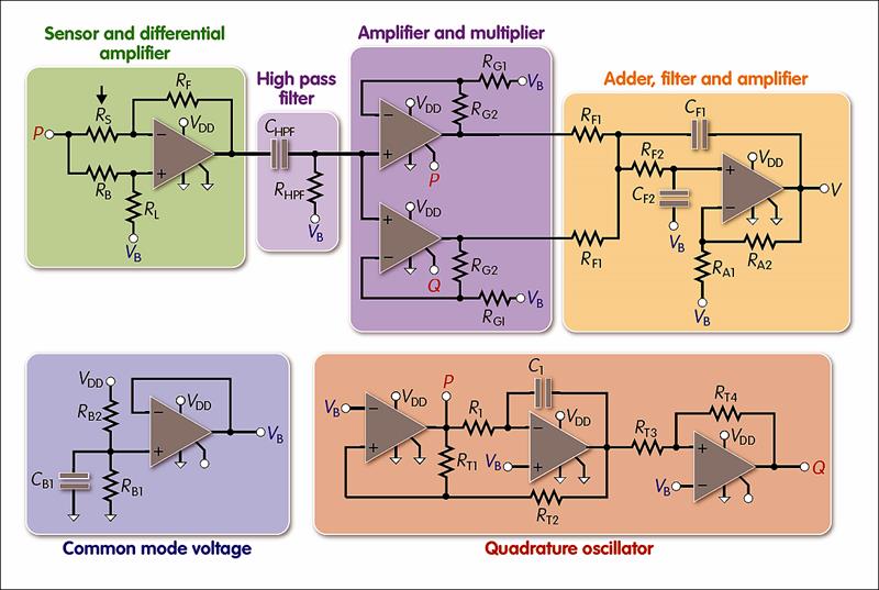
A proposed lock-in amplifier circuit is shown in figure 1. The quadrature oscillator generates two phase shifted pulsed voltage signals; P (in phase) and Q (in quadrature). The in phase signal is also used to power the sensor.
The signal from the sensor is amplified by the differential preamplifier and then brought to the inputs of amplifier and multiplier, where it has been amplified – using three relatively low gain amplifiers in order to maintain a large bandwidth – and multiplied by the in phase and in quadrature signals. After the multiplications, the signals are added to eliminate the possible phase shift of the sensor. After a low-pass filter stage and amplification, the output signal Vout is proportional to the measured physical quantity.
In order to meet these requirements, the circuitry can be created using the Silego SLG88104 quad op amp. The complete circuit requires eight op amps (two SLG88104 chips), along with a small number of passive components.
Due to the phase-sensitive detection ability of the lock-in amplifier, the output voltage signal will provide precise information about the measured physical value, even with high levels of noise. It is worth mentioning that these op amps are sufficient for the complete design, even in the case of multiplication, where analogue multipliers or switches have been used.
Using the SLG88104 for this application offers several advantages. First, it has a relatively low corner frequency of flicker noise, estimated from the datasheet to be approximately 0.7Hz. This allows the use of a quadrature oscillator frequency of about 100Hz (where the noise floor has been reached) and the use of large resistors in the design and thus low power consumption.
A low oscillating frequency means the corresponding amplifiers can have relatively large gains, as the op amp’s gain-bandwidth product is 10kHz. Another important feature is the possibility of powering down the SGL88104 by using the PDi (i = 1, 2, 3, 4) inputs. This allows multiplication of the signal at the differential amplifier’s output and the corresponding P and Q signals from the pulsed quadrature oscillator.
The input to the lock-in amplifier typically depends on the type of sensor used. For example, in figure 2, a resistive sensor (Rs) is used. This type of sensor changes its resistivity when some physical parameter such force, pressure or temperature, acts upon it. The output of the lock-in amplifier is a voltage signal proportional to the measured physical value.
Circuit elements
* Common mode voltage
The suggested circuitry has a single power supply (VDD) of 3V. This can be created using two standard 1.5V batteries connected in series. In order to make a full span of the output voltage, the common mode voltage must be 1.5V, so resistors RB1 and RB2 must have the same large values, in this case 1MΩ. Capacitor CB1, which filters the noise, must also have a large value and it is suggested that CB1 is realised by connecting two capacitors with values of 100μF and 220nF in parallel.
* Quadrature oscillator
This generates two pulsed, phase shifted voltage signals for gating the corresponding op amps. In order to reduce power consumption, resistors RI, RT1, RT2 and RT4 must have large values. In the suggested design, RT1, RT2 and RT4 are set at 1MΩ, while RI = 700kΩ. To keep the oscillating frequency near to 100Hz, CI should be 2.2nF.
In order to reduce the hysteresis of the Schmitt trigger and the additional phase shift of the in quadrature signal, RT3 should be 1kΩ.
* Differential preamplifier
As power consumption is a major concern, the values of the resistors RF and RL have been chosen to be 1MΩ.
The values of resistors RS – the sensor – and RB must be chosen such that the differential preamplifier can amplify a pulsed signal with a frequency of more than 100Hz without distorting it. Therefore, the optimal values of resistors RS and RB are approximately 100kΩ. This design results in a bandwidth of approximately 1kHz.
* High pass filter
The differential preamplifier output consists of a slow varying part, proportional to the common mode voltage VB, and a fast varying part proportional to in phase signal P. The high-pass filter removes the slow varying signal, the offset voltage and low frequency flicker noise from the differential amplifier.
In order to achieve a cut-off frequency of about 1Hz and a low output current, CHPF is set at 220nF and RHPF at 1MΩ.
* Amplifier and multiplier
The amplifier and multiplier stage amplifies the signal from the high pass filter and performs digital multiplication by gating the op amps. In order to achieve relatively high gain without distorting the signal, while minimising power consumption, the following resistors value have been chosen – RG1=100kΩ and RG2=1MΩ.
* Adder, filter, and amplifier
This stage has a triple role – to sum the output signals of the amplifier and multiplier, to perform low-pass filtration and, additionally, to amplify the signal. The sum of the signals occurs at the common node of the resistors RF1 and RF2, which also serve as the low-pass filter components.
In order to keep low power consumption, sufficient amplification and filtration with the second order Butterworth filter, which has a cut off frequency of approximately 1Hz, the following values should be used: RA1=100kΩ, RA2=1MΩ, RF1=2MΩ, RF2=1MΩ, CF1=56nF and CF2=390nF.
Conclusion
The most prominent feature of the lock-in amplification is the suppression of the high levels of low frequency flicker. The aim of the above presented measurements is to prove the concept of such a designed lock-in amplifier.
The ultra-low power low voltage lock-in amplifier circuitry described above is capable of providing high performance measurement that offers phase sensitive measurement. Flicker noise, which is the predominant noise component in any sensing system aimed for measuring slowly varying physical values such as temperature, force and pressure, is effectively suppressed by the suggested design.
The introduction of this low voltage, ultra-low power measurement system, which can be easily battery powered, opens broad new applications. Furthermore, the circuitry can be used with different types of sensors in order to prove the concept of the circuit design. Moreover, the result of this test can be used in order to improve the design in a way to reach higher-precision and wider bandwidth. Finally, by choosing larger resistor values, power consumption can be further reduced, with the trade off being increased noise and lower measurement resolution.
Author profile
Lazo Manojlović is a Professor at the Zrenjanin Technical College.
Open the pdf to access the full version of this article.


