
SD converters operate on two principles – oversampling and noise shaping. In general, and for a given band of interest, the dynamic range improves by 3dB for every oversampling factor of 2, assuming a white noise spectrum. Meanwhile, the noise transfer function shapes the noise to higher frequencies, further reducing quantisation noise at the band of interest.
However, one disadvantage of oversampling is the requirement for an input buffer to drive the SD modulator may become more stringent than for architectures operating at lower sampling frequencies. Moreover, presenting a very high input impedance with high precision to the sensing element is critical for measurement accuracy in sensing systems. This makes the requirement for input buffers even more critical.
Integrating an input buffer generates other challenges. The SD modulator offers very low noise at low frequencies, but any additional component – such as the input buffer – will add thermal noise and, more importantly, flicker noise at low frequencies.
In addition, the buffer’s offset may contribute to overall system error. This can be compensated for by system calibration, but if offset drift is relatively high, this approach may be impractical.
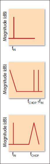 These two problems are typically solved by chopping the buffer’s inputs and outputs. In this way, input frequency is modulated to higher frequencies, while buffer offset and flicker noise remain at their original low frequencies as they are not affected by the input chopping (see fig 1a).
The output dechopper mechanism demodulates the input frequency back to baseband, which modulates the offset and flicker noise added by the buffer to higher frequencies that will be removed by the A/D converter’s low pass filter.
In some cases, the input buffers are replaced by a resistor based instrumentation amplifier (resistive PGA) to accommodate a small sensor signal to the full modulator input range, maximising dynamic range. A resistor based instrumentation amplifier is preferred over a differential resistive amplifier, due to the higher input impedance required in discrete sensors (see fig 1b).
The main restriction in using this amplifier topology is the limitation on the common mode voltage, especially with gains other than unity; the resistive PGA has a floating common mode that depends on the input signal.
Resistive network mismatch and its drift is a concern in the overall error budget as it may have an impact on most of the precision specifications.
To avoid these limitations, recent SD converters from Analog Devices have employed a capacitive PGA, where the gain depends on the capacitor ratios (see fig 2).
In order to amplify DC signals, the capacitive PGA introduces a chopping mechanism at the PGA inputs; the DC input signal is modulated to the chop frequency, then amplified by the capacitive amplifier. Finally, the signal is demodulated back to DC by the output dechopper. Amplifier offset and flicker noise is modulated to the chop frequency and low pass filtered at a later stage.
There are some benefits associated with this approach:
* Better noise versus power trade-off as there are fewer noise sources.
* Capacitors offer a range of advantages over resistors; apart from being noiseless, they don’t suffer from self heating and normally offer better matching and temperature drift
* The capacitors decouple the input common mode from the rest of the signal chain common mode. This offers an advantage in terms of CMRR, PSRR and THD.
* The capacitive PGA input common mode range may be rail to rail and beyond.
This capacitive architecture combines the benefits of an instrumentation amplifier –which has a really high input impedance as the input impedance is a capacitor – with the benefits of capacitors over resistors as the gain element. This increases the amplifier’s dynamic range, not only in terms of signal swing, but also noise efficiency.
In a Wheatstone bridge, common mode voltage is defined by the impedance connected in each leg and proportional to the power supply. Weighing scale applications implement this sensing topology due to the benefit of linear sensing.
Strain gauge sensitivity is typically 2mV/V and the higher the Wheatstone supply, the higher the sensitivity. To increase the strain gauge’s dynamic range and maximise the signal to noise ratio, the bridge may be powered at higher supplies than the A/D converter.
In a resistive PGA, common mode limitation means the bridge should be powered at the same voltage as the A/D converter. However, it can be powered at almost twice the A/D converter supply voltage in a capacitive PGA as there is no input common mode limitation.
When powering the converter at 3.3V and assuming a buffer headroom of 100mV, the improvement in dynamic range of a capacitive PGA over a resistive PGA for the same selected gain could be 5.2dB.
Another example is temperature measurement using resistance temperature detectors (RTD) or thermocouples. A popular RTD resistor, such as the PT100, may be used to sense temperature directly or to sense the cold junction of a thermocouple indirectly.
A conventional way to measure the temperature while cancelling the lead error in a three wire RTD configuration is shown in fig 3a. Here, the internal current sources of the AD7124-8, drive two wires of the RTD with the same current, generating an offset error equal in both leads and proportional to the lead resistance.
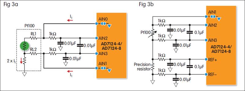
Due to the small value of the lead resistance and the currents provided by the AD7124-8 to minimise the self heating effect, the offset voltage generated is close to the negative rail. This reduces the maximum allowable gain in a resistive PGA significantly as its input common mode would also be close to the rails. A capacitive PGA will set the common mode voltage internally to half of the supply rails, allowing for a higher gain configuration and increasing overall dynamic range.
The proposed solution reduces system complexity and hardware connections, as the third cable may not be returned to the converter’s PCB and can be connected to ground near the RTD.
To increase precision, four wire measurements are preferred. In this case, only one current reference is used. To avoid imprecision on the current source, ratiometric measurement can be used, with a precision resistance used as the A/D converter reference voltage generator (see fig 3b).
For a 3.3V supply in a resistive PGA, the voltage generated on the precision resistance should be around 1.65V, otherwise the PGA common mode voltage will limit the maximum gain. The consequence is the maximum gained signal should be equal to 1.65V.
In a capacitive PGA, there is no input common mode limitation, therefore the RTD common mode signal can sit close to the top rail. This allows the A/D converter reference voltage generated by the precision resistor to be maximised and, hence, the highest selectable gain and dynamic range.
Author profiles:
Miguel Usach is an applications engineer, Gerard Mora-Puchalt is an analogue IC designer engineer. Both are with Analog Devices.


