
A whole range of new use cases is also on the horizon, such as augmented reality (AR) and virtual reality (VR), autonomous vehicles, and remote surgery, for which ultra-low latency will be required. At the other extreme, massive machine-type communications (MTC) for the Internet of Things (IoT) will largely not require wide bandwidth or low latency, but the sheer volume of connected devices would be too much for conventional cellular networks to cope with.
Fixed wireless access, where 5G would be used to provide high-speed Internet connectivity to regions where fibre is uneconomic, is already proving to be a popular proposition as an early application. The conflicting needs of the different use cases would be met by ‘network slicing’, which will allow different parts of the virtualised network to be optimised for each application.
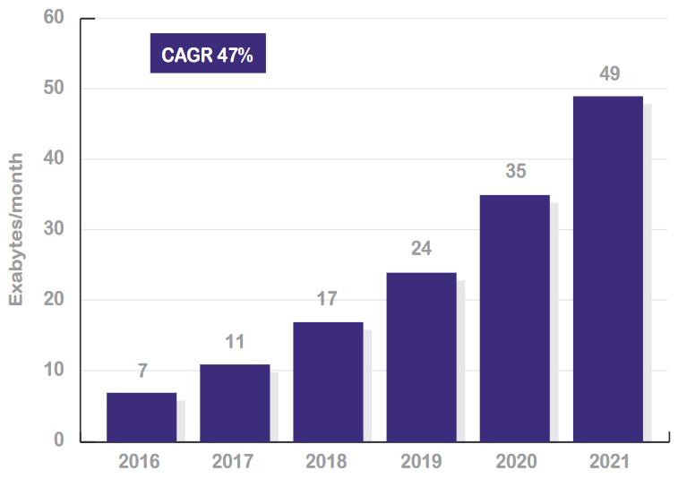
According to Cisco, global mobile data traffic grew an estimated 63% in 2016, and is predicted to grow at an average rate of 47% over the succeeding five years to reach 49 exabytes (1018) per month by 2021, see Figure 1. Even existing applications, such as the use of smart devices, are accelerating rapidly, with a 300% increase in mobile payments and 40% of cars forecast to be ‘connected’ by 2020, and also 560m wearable devices in use by 2021. HD video streaming, which is already challenging 4G networks, will evolve to 4K and then 8K, massively increasing the demand for bandwidth. 5G is also intended to provide the foundation on which to build smart cities, pushing mobile network performance and capability requirements to the limit.
In order to meet these demands, the International Telecommunications Union (ITU) has set ambitious target specifications for 5G network performance, as shown in Table 1. The networks are being designed to be able to provide 100 billion connections worldwide.
This level of performance presents some serious economic and engineering challenges, as well as potentially some excellent opportunities for UK companies to take a lead. The UK is home to two important 5G testbeds: the 5G Innovation Centre (5GIC) based at the University of Surrey, and the University of Bristol 5G Testbeds and Trials Programme. It has been estimated that this research could enable an additional £173billion to the UK economy by 2030.
Figure 1: The forecast growth in global mobile data traffic from 2016 to 2021. Source: Cisco
In order to deliver 5G services, some radical new technologies are needed. For the first time frequency bands in the millimetre-wave (or mmWave) spectrum above 24GHz, will be used for cellular access. These frequencies have been used for some time for wireless backhaul, to connect base stations to the backbone network, but up to now they have not been used in handsets or the base stations themselves. Because of the propagation characteristics of mmWave signals it will be necessary to deploy ultra-dense cellular networks with base stations around 250m apart, meaning that in an urban environment many lampposts will probably carry a mmWave base station.
Despite the complexity of working in this frequency range, the sheer number of base stations will necessitate a reduction in unit cost, while delivering improved bandwidth, power and efficiency compared with today’s macro base stations. A corresponding increase in the number of backhaul radio links will also be seen.
In addition to the densification of conventional base stations, other types of delivery platform are being considered, which may include low earth-orbit (LEO) satellites, high-altitude platforms (HAPs) or even drones, all of which will need RF technology.
Gallium nitride (GaN) is already rapidly emerging as the semiconductor material of choice for use in 4G base station solid state power amplifiers (SSPA), due to its high electron mobility, coupled with typical transition frequencies (fT) of 200GHz. This, along with its high breakdown voltage and high thermal conductivity, enable it to deliver power levels in tens of watts under linear operating conditions. Already around 40% of 4G base stations use GaN power amplifiers, according to US manufacturer Wolfspeed. The more demanding bandwidth, power efficiency and linearity requirements of 5G will mean that GaN will dominate those base station SSPA slots, initially in the sub-6GHz bands but later at mmWave frequencies.
Although GaN devices are currently more expensive to fabricate than those using other substrate materials, such as gallium arsenide (GaAs) and silicon, increasing volumes and wafer sizes could reduce costs.
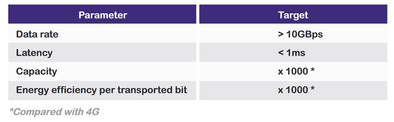
Table 1: The International Telecommunications Union has set ambitious targets for 5G network performance. Source: IMT 2020
The EPSRC Hub for future manufacturing of compound semiconductors, hosted at Cardiff University, is researching ways to fabricate compound semiconductors on silicon substrates with a view to driving down the manufacturing costs. It is hoped that this research will yield advances in heterogeneous integration, in which GaN and silicon devices could be integrated onto the same chip to make the best use of both materials.
In order to fully exploit the properties of GaN, improvements are required in the materials and processes used to make the chips themselves and to build the SSPAs and systems that use them.
Many of the challenges relate to providing adequate heatsinking and thermal management for the devices, which are able to run at much higher channel temperatures – typically up to 400˚C – than either silicon or GaAs. Other challenges include developing new low-loss printed circuit materials and manufacturing techniques for the high-volume production of subsystems using GaN devices, including the potential of 3D printing microwave circuits and nano-scale metamaterials. Many universities and technology companies in the UK have skills and research interests in these areas, and Innovate UK is keen to stimulate and encourage the advancement of this indigenous capability.
Development kits
In many branches of electronics, development kits are often used to evaluate the performance of new chips, as a means of shortening the time required to take a product to market. Development tools and evaluation boards have traditionally offered an easy way to explore the applications of a product without the need to manufacture a custom circuit. This approach is equally applicable to new GaN devices.

Development kits form a key strategy of the recently-announced Compound Semiconductor Applications Catapult. This Catapult plans to launch a series of development kits in the areas of power electronics and photonics as well as RF and microwave. The development kits will be produced with support from UK companies, and where possible will feature chips from UK foundries. Companies will be able to use these development kits to explore new applications, and to launch products that will drive sales for companies across the UK supply chain.
"Development kits will be produced with support from UK companies and, where possible, will feature chips from UK foundries."
Dr Andy Sellars
As a result of a number of workshops where the Catapult has consulted relevant companies, several categories for prospective compound semiconductor (GaAs and GaN) development kits have emerged:
- mmWave SSPA modules and transceivers and antennas for automotive, 5G and satellite communications applications
- 100W, 6 to 30GHz compact SSPAs for space and defence
- Low power (up to 100mW), high efficiency power amplifiers at 0.8 to 5GHz for IoT applications
- Sub-6GHz SSPAs for 4G LTE and 5G base stations, integrating software defined filters, active antennas, and switches
- THz power amplifiers for security and medical applications
- Direct RF to digital and digital to RF conversion: 10GHz D/A and A/D converters, eliminating IF stages and providing digital reconfiguration.
The consultative process is continuing, and the Catapult welcomes further suggestions from UK companies for development kits that would help to stimulate the already outstanding capabilities of the RF supply chain and equip them for the future.
A particular challenge is to reverse the decline in RF compound semiconductor chip production in the UK: our indigenous chip design and prototyping expertise is world class, but most fabrication currently takes place using overseas foundries.
Working with the UK’s fabless chip designers, the Catapult has ambitions to commission new RF chips from UK foundries for inclusion on development kits.
Author profile:
Dr Andy Sellars is chief business development officer with the Compound Semiconductor Applications Catapult


