Yet there is a growing push to democratise chip design: bringing it to a wider community of engineers, both professional and amateur. This may seem an impossible task but the movement is working on much older technologies as they gradually become more accessible.
It is nowhere near as dramatic as Moore’s Law for high-volume chips but the silicon learning curve works for mature processes as well, particularly for the upfront costs such as mask making. At introduction, a full mask set for the 180nm process could easily cost $300,000 and ran to more than half a million dollars for 130nm. Today the picture is quite different. The Global Semiconductor Association’s industry survey found over the past two years, 180nm mask-set prices were no more than $60,000 and often below $80,000 for 130nm sets.
Even before mature-process masks fell in price, one low-cost way into ASIC prototyping and even low-volume manufacture lay in the multi-project wafer (MPW) or ”shuttle”, to use the name favoured by foundry TSMC. This takes advantage of the differential between the size of most commercial integrated circuits (ICs) and the area of the reticle that the lithography tool uses to print features on the surface of the wafer. You can get a lot of designs that take up 10 to square millimetres on a reticle that may measure 600 square millimetres. On the other hand, the number of chips you can opt receive may be limited to just a few dozen but potentially enough to get a project to the point where external funding is an option.
The mask set is far from the only upfront engineering cost. Tools and IP are vital for any design, which at the higher end easily run into millions. One option for cash-poor designers lies in lower-cost tools, such as the Tanner suite sold by Siemens Digital Industries Software and IP. Arm, for example, rejigged its DesignStart programme earlier this month, offering access to a selection of its microcontroller-oriented cores without demanding an upfront licence fee, just royalties after production.
Other activities mirror what has happened in many parts of software development with projects such as Eclipse: build a design environment around open-source tools. Many chip-design teams are using open source in part already, through the modelling language SystemC as well as the Python programming language, which has found favour for controlling the test harnesses used in RTL verification.
Opensource initiatives
A potentially important initiative is US research agency DARPA’s OpenRoad initiative, with aims to build a more comprehensive set of open-source design tools. Professor Andrew Kahng of the University of California at San Diego and principal investigator on the project envisages an environment that can lay out and tune a range of chip designs automatically through a combination of machine learning and what he calls “extreme partitioning”, which divides the chip into many small independently optimised modules.
Though verification engineers have embraced various forms of open source, the stumbling blocks for its adoption get bigger the closer you get to tape-out. The biggest issue lies in the process design kits (PDKs) provided by foundries that are jealously protected by non-disclosure agreements and which forbid any sharing.

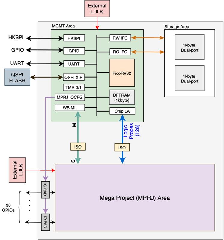
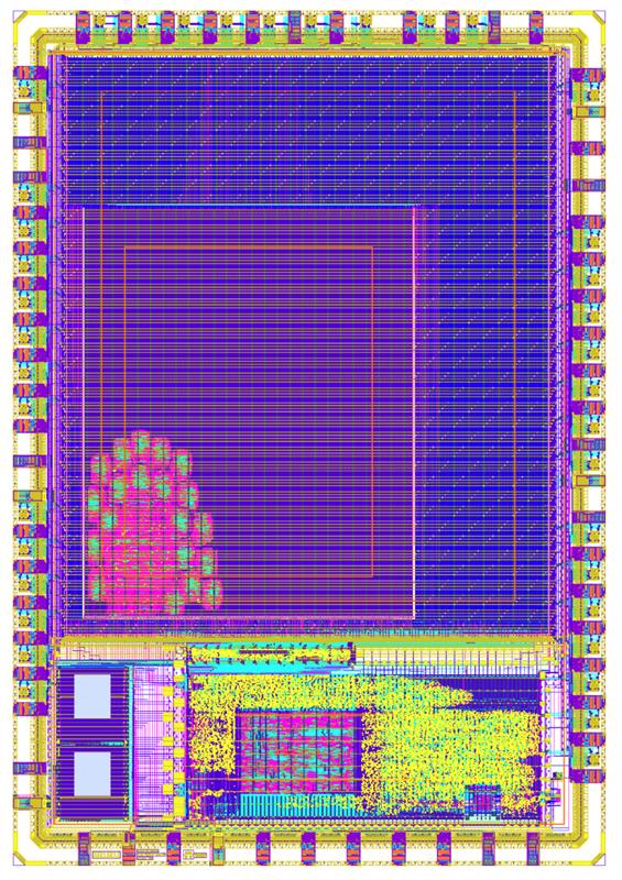
Figures above and below: The Caravel test infrastructure, developed by Antmicro, provides a ring of I/O and test ports administered by a built-in RISC-V core
 For an example of the issue during a seminar organised by the IEEE’s Solid-State Circuits Society, Google software engineer Tim Ansell pointed to the Ravenna RISC-V microcontroller developed by Efabless, a start-up that is trying to establish a marketplace of open-source IP and silicon. The microcontroller was made on X-Fab’s XH018 process is an open-source design except for the physical layout, which uses the foundry’s PDK and analogue IP.
“Efabless was unable to release a completely reusable result,” Ansell notes. “Someone like me couldn't look at how something was implemented in the gates. There is a problematic attitude in this industry around sharing.”
Ansell says Google is keen on the ability to share knowledge on the basis that it accelerates progress in general. “With Moore’s law slowing down new innovative solutions will be needed to keep up with the ever growing demand for computation,” he adds.
Providing a wider community with access to silicon design may provide avenues for creating novel methods for computation that are less likely to come about through traditional R&D. To help push that forward, Ansell started trying to convince foundries to open up their PDKs. “I talked to a lot of foundries. And I got laughed at by a lot of foundries.”
One foundry did come round to the idea: Skywater, a company operating a fab in Minnesota owned by Cypress Semiconductors up to a few years ago. “We were able to come to an agreement that allowed us to release a 130nm PDK under an open-source licence,” Ansell says. Downloadable from Github, the PDK uses an Apache 2.0 licence and can be cloned by any user “without having to ask my permission or having to ask Skywater's permission. An open-source PDK means we can have fully open-source ASICs.”
Google and eFabless then set about building an MPW service that extends the possibility of ASIC design to people without the tens of thousands of dollars to get something back from the fab. To qualify for the free chips, designers need to be prepared to not just make their own designs open source they also need to be prepared to deliver samples to users who are interested in working with the design and the resulting silicon. “Your design has to be open source all the way down to the GDS,” Ansell says.
The shuttle will returns around a hundred samples, which Ansell sees as a high-enough number for users to not worry about providing other users with silicon on request and try to deliver on the sharing possibilities of open-source hardware. “Open source makes it easy for people to collaborate. This allows people to attempt things that they used to think were too risky. It makes it easy and cheap to fail, and to learn from your failures.”
Constraints
A further constraint is the requirement to use the Caravel test infrastructure developed by Antmicro. This provides a ring of I/O and test ports administered by a built-in RISC-V core. “If you are building a test chip to begin with, you need something like this,” notes Efabless CTO and co-founder Mohammed Kassem. In the middle of this I/O ring is a 10 square millimetre hole for the user’s custom silicon that can be used for anything without payment.
Though the area is relatively small, Ansell says complex digital designs are achievable as the 130nm can deliver more than 1.5 million gates. ”People vastly underestimate the digital capabilities of older nodes because they are mostly used these days to target low power and analogue designs,” he notes.
Submissions for the first run at Skywater on the 130nm process closed in November 2020 and the second closes for submissions in mid-June, with parts to be delivered from that second run to project owners in early December. Google is funding six of the shuttles in the near future. Efabless also offers paid-for MPW to design teams that do not want to commit to the fully open-source hardware route.
The first shuttle included designs from companies such as IBM and Quicklogic.
“But the most exciting thing was that 60 per cent of the designers have never done an ASIC before,” Ansell says. “The success of the SkyWater programme shows that a huge demand exists for open solutions and we now have had some initial interest from other foundries.”
While work on advanced nodes pushes design costs ever higher, though with potentially huge rewards when the resulting chips go into production, work at the trailing edge on democratising design may prove equally important to driving progress in the industry.


