
Many wireless electronic systems operate over wide frequency ranges and the need for more bandwidth continues. As a result, the systems engineer faces challenges trying to design electronics to cover the entire frequency range.
Given the possibility of having one signal chain cover the entire frequency range, most systems engineers would get excited at the prospect. However, the one signal chain approach is always related to the performance degradation that comes with a wideband solution vs. a narrow-band solution. At the heart of this challenge is the power amplifier, which commonly has superior performance when tuned over a narrow bandwidth.
Traveling wave tube (TWT) amplifiers have dominated higher power electronics as the output power amplifier stage in many of these systems. However, given the long-term reliability of semiconductor ICs, there has been a push toward these electronics, starting with GaAs. The emergence of GaN technology operating at 28V to 50V on a low loss, high thermal conductivity substrate like silicon carbide (SiC) has now opened up a range of new possibilities.
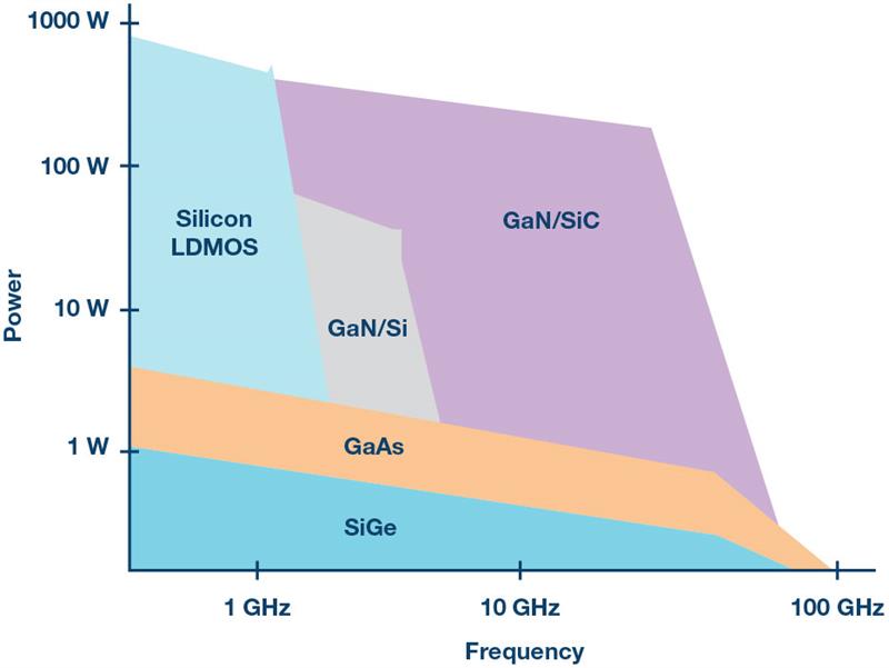
| Figure 1: A process technology comparison of microwave frequency range power electronics |
Today, GaN on silicon technology is limited to operation below 6GHz due to the RF losses associated with the silicon substrate and its lower thermal conductivity.
The emergence of GaN technology has created a move toward GaN amplifiers as the output stage of these systems. The driver amplifier in many of these systems is still commonly GaAs. So, how do you use circuit design to extract as much power, bandwidth, and efficiency out of these wideband power amplifiers?
Certainly GaN-based designs are capable of higher output powers than GaAs-based designs, and the design considerations are largely the same.
Design considerations
The most common type of monolithic amplifier design is a multistage, common-source, transistor-based design, also known as a cascade amplifier design. Here, the gain multiplies from each stage, leading to high gain and allows us to increase output transistor sizes in order to increase the RF power.
GaN offers benefits here because engineers are able to greatly simplify the output combiners, reducing loss, and improving efficiency, as well as shrinking the die size, making wider bandwidths and improved performance possible.
A less obvious benefit of going to GaN devices is to achieve a given RF power level, perhaps 4W - the transistor size will be less, resulting in a higher gain per stage. It will lead to fewer stages per design and ultimately, higher efficiency. The challenge with this cascade amplifier technique is that it is difficult to achieve bandwidths over an octave without significantly compromising the power and efficiency.
One approach to achieve wide bandwidth design is to implement a balanced design with Lange couplers on the RF input and output. The return loss is ultimately dependent on the coupler design, as it becomes easier to optimise the gain and power response over frequency without also needing to optimise the return loss.
Another topology to consider is the distributed power amplifier which incorporates the parasitic effects of the transistor into the matching networks between devices.
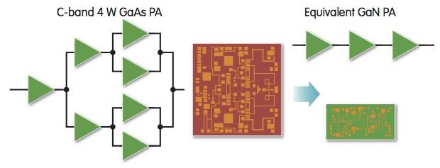
| Figure 2: Comparison of multistage GaAs PA vs. an equivalent GaN PA |
The input and output capacitances of the device can be combined with the gate and drain line inductance, respectively, to make the transmission lines virtually transparent, excluding transmission line loss. By doing this, the gain of the amplifier should only be limited by the transconductance of the device and not the capacitive parasitics associated with the device. This only happens if the signal traveling down the gate line is in phase with the signal traveling down the drain line, so that each transistor’s output voltage adds in phase with the previous transistors output. The signal traveling to the output will constructively interfere so that the signal grows along the drain line. Any reverse waves will destructively interfere since these signals will not be in phase. The gate line termination is included to absorb any signals that are not coupled to the gates of the transistors. The drain line termination is included to absorb any reverse traveling waves that could destructively interfere with the output signal and improve the return loss at low frequencies. As a result, multiple decades of bandwidth are able to be realised from kHz to many GHz. This topology is popular when more than an octave of bandwidth is needed and there are some nice benefits, such as flat gain, good return loss, high power, etc.
One challenge with distributed amplifiers is that the power capability is dictated by the voltage applied to the device. Since there is no narrow-band tuning capability, you are essentially providing a 50Ω impedance to the transistor or close to it. Therefore, the achievable output power is set by the voltage applied to the amplifier such that if we want to increase the output power, we need to increase the voltage applied to the amplifier.
This is where GaN becomes very helpful, as we can quickly go from a 5V supply voltage with GaAs to a 28V supply voltage in GaN, and the achievable power goes from 0.25W to almost 8W, simply by changing the technology. There will be other considerations to look at such as the gate length of the process available in GaN and if they can achieve the gain you need at the high frequency end of the band.
The fixed RL of 50Ω for distributed amplifiers is different compared to the cascaded amplifier where we change the resistance value presented to the transistor by matching networks to optimise the power from the amplifier. There is a benefit in optimising the resistance value presented to the transistor with cascade amplifiers in that it can improve the RF power. Theoretically, it is possible to continue increasing the transistor periphery size to continue increasing the RF power, but there are practical limitations to this, such as complexity, die size, and combining loss.
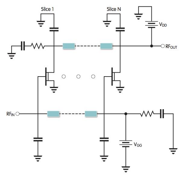
| Figure 3: A simplified block diagram of a distributed amplifier |
The matching networks also tend to limit the bandwidth, as they become difficult to provide an optimum impedance over wide frequencies. In the distributed power amplifier, there are only transmission lines whose purpose is to have the signals constructively interfere along the amplifier, rather than matching networks.
There are additional techniques to further improve the power in distributed amplifiers, such as using a cascade amplifier topology to further increase the voltage supply to the amplifier.
Each of these different topologies and technologies have a place in the semiconductor world, as they each provide benefits, which is why they have survived to this day.
The emergence of new semiconductor materials like GaN have opened the possibilities to reach higher power levels covering wide bandwidths.
Shorter, gate length GaAs devices have extended frequency ranges from 20GHz to 40GHz and beyond. The reliability of these devices is shown to exceed 1million hours, making them ubiquitous for modern day electronic systems.
It’s to be expected that the trends of higher frequencies and wider bandwidth will continue into the future.
| Author details: Keith Benson is product line director for RF/microwave amplifiers and phased array ICs, Analog Devices |


