
This degree of miniaturisation is taking packaging technology beyond what can be achieved using SMT assembly. “Now, designers are having to create hybrid solutions,” Bergman contended.
“It’s not just integrating digital and analogue devices,” he continued, “it’s also about the integration of things like mechanical components, optics and flexible circuits.”
ASE Group has been in existence for more than 30 years and is a leading provider of outsourced semiconductor assembly and test. According to Bergman, the trend towards hybrid solutions, whilst picking up pace more recently, started to manifest itself about a decade ago. “Chip makers began to find it difficult to sell singly packaged chips because of the tuning needed. They found it easier to include things like passives and inductors in the package.
“But that solution is still an SiP and a component level solution driven by the chip makers themselves.”
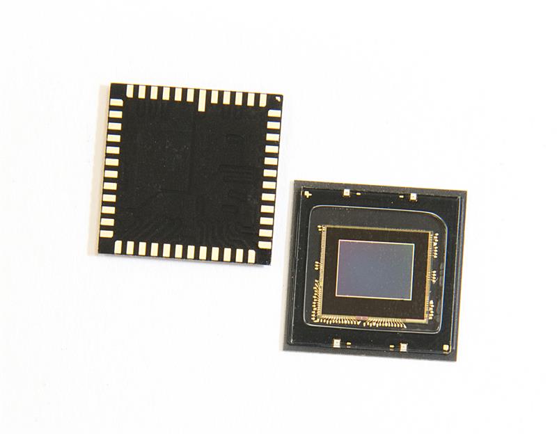
Today’s solutions are modules, he asserted. “Take a camera module for a mobile phone,” he said. “It’s a small cube with a flexible connector attached. But it includes a MEMS device, piezo devices for image stabilisation, a lens stack, an image processor and, probably, power management.
“Creating those modules is what ASE is focused on. We’re enabling customers to get the best of ASE and partner company Universal Scientific (USI) for the next generation of innovation.”
Not surprisingly, Bergman pointed towards the mobile phone as one of the first devices to take advantage of modules. “A single handset today can have 10 or 15 sensors and these need to be reduced to the smallest size possible on an individual basis. But ASE is now providing more functionality by combining multiple sensors with, for example, a microcontroller or another type of processor – we’re creating sensor fusion modules because it’s all about space and functionality.”
 While modularisation is the goal, there is still the need to apply some rules. “We try to keep common elements together,” he said. “For example, we would put inertial sensors like gyros and accelerometers together, but we might not combine an accelerometer with a pressure sensor.”
However, whilst some sensors might not be grouped, there is a move to integrate optical sensors into these modules.
Bergman pointed to smartwatches and similar wearables that measure a heartbeat. “The optical sensor measures the user’s pulse, but accuracy is affected by movement of the wrist. So some modules will now include an accelerometer to analyse the motion and cancel out false signals.”
And MEMS is playing a central role in enabling these modules to be created. But it’s not just integration, as Bergan explained. “In broad terms, we’re moving to a connected world, with artificial intelligence, virtualisation and so on. This will need tight integration of hardware, software and content if it’s to work and if the developer is going to differentiate themselves from similar devices. Many developers have the software and the content; what they want now is the hardware.”
In Bergman’s opinion, hardware is, essentially, an I/O device. “The sensors are inputs, there’s outputs to a network and an interface to the user.
“But it’s not just phones and wearables; things like Amazon Echo have MEMS microphones.”
ASE, however, is not a device developer; it’s a manufacturer. “But USI does have system level design and test expertise for integration,” Bergman pointed out. “In many cases, we will work with a company looking for some functional blocks. It will come to us and provide specifications. USI will do an ODM design and then produce a module, so we can provide package level and subsystem design in this way.”
And ASE says its package design expertise is increasingly relevant for MEMS devices. “There are a number of factors which need to be kept in mind,” Bergman said. “Stress management is the most important as many MEMS parts feature thin moving elements made on fine geometries; any stress can impact device performance.
“When you package MEMS designers, you have to be careful about how the package is moulded and the stress introduced by the various coefficients of expansion.”
Stress, however, is only one parameter. “If you’re dealing with MEMS devices which need to interact with the environment – a pressure sensor or a VoC sensor – the chip needs to be exposed. And it’s the same with optical devices,” Bergman added. “How do we provide adequate shielding
without impacting performance?”
One market which Bergman says is becoming ‘interesting’ is automotive. “Until now, automotive has used MEMS for safety; now, there is a move to use them as management devices. But how do you assure the performance and accuracy of a device in such a pressured environment? How much redundancy will be needed for ADAS, for example?”
The result of these factors is that ASE is now doing more modelling and simulation, for factors such as stress, thermal performance and electrical performance. “In MEMS, however, it’s mainly for stress.”
Devices now being developed require a deeper level of discussion to make sure the solution will be successful. “But there are always things that crop up in manufacturing,” Bergman accepted. “Customers continue to push technology and we find new wrinkles. So there’s more collaboration, joint development and risk assessment up front to work out what it is we have to do,” he concluded.
MEMS Tech Showcase finalists announced The finalists have been announced for the MEMS & Sensors Industry Group’s annual Tech Showcase, taking place during the group’s Executive Congress. The finalists are:
|


