
In the three decades since that submission, the technology has developed from being an academic curiosity to being an almost essential part of daily life.
The list of applications is impressive, ranging from sensors in cars which deploy the airbags in case of a collision, nozzles of ink jet printers, sensors and, more recently, the so called 'lab on a chip'.
But these devices have been based on one premise; detecting the movement of a cantilever and amplifying the signal produced. They have also taken advantage of the techniques used to create semiconductors. Because there is no imperative to rush to the 'bleeding edge', MEMS devices continue to be made on trailing edge processes and take advantage of the economics of those processes.
Almost in parallel, a number of organisations were developing micro optical systems. In the mid 1990s, the two technologies began to converge and the phrase 'micro opto electromechanical systems' – or MOEMS – appeared. However, devices based on the approach have only appeared on the market in the last couple of years.
One of the companies offering MOEMS based parts is Hamamatsu. Jack Bennett, a sales engineer with the company's UK operation, noted: "MOEMS is obviously a development of MEMS technology; and there are a lot of MEMS parts out there. But MOEMS adds an optical element, which could be something like a lens, but could also be a detector technology, such as a photodiode. There is also the opportunity to integrate things like moving mirrors into a system."
While many will interpret the acronym MEMS as meaning a product, Bennett pointed out that it also relates to the manufacturing process. "There are a lot of fabrication techniques involved in making MEMS devices, including bump bonding, back thinning of CCDs, nano imprinting, etching and, more recently, through silicon vias."
He believes the development of MOEMS technology will enable designers to apply a lot more creativity. "The devices themselves are more interesting," he contended. "Looking at the 'big picture', a lot of MOEMS devices in the near future will look a lot like today's MEMS parts, but will feature a detector of some kind. However, in the future, I think we'll see a lot more integration of optical components – even lasers. Eventually, the devices will progress to take advantage of nanotechnology, creating nano opto electromechanical systems – or NOEMS."
Hamamatsu, which has been developing MEMS devices for the last decade, is likely to follow the trend, according to Bennett. "The company's solid state division will move from supplying detection devices to supplying more integrated products. While it's a small part of Hamamatsu's business, it's big in terms of the investment in R&D and so on. The business will grow considerably over the next few years."
In fact, Hamamatsu said in 2014 that it had completed the construction of a facility in Japan for the development and mass production of MOEMS based devices and modules. According to the company, the site will produce parts for use in automotive, smartphone and other applications.
While Hamamatsu will continue to make MOEMS devices in Japan, it has recently established a European Innovation Centre in Switzerland. "This centre is being directed by Professor Peter Seitz, who is well known in the field," Bennett said. "It's a special group which can design things quickly."
Bennett sees the launch by Hamamatsu of MOEMS devices as 'exciting'. "They will allow designers to make smaller products," he said.
One of the areas which Bennett believes MOEMS will enable is portable products. "A lot of today's MEMS based devices aren't designed to replace things like benchtop instruments. While a benchtop interferometer might cost more than $10,000, a MEMS based version might be available for $1000. But while it might be cheaper, it may not be as sensitive.
"But MOEMS devices will create a new industry," he continued, "and we envisage portable applications such as IR spectroscopy and air quality measurement. MOEMS will give people the opportunity to develop new solutions, rather than updating existing ones."
One area which Bennett sees as attractive is small, affordable health care devices. "In the near future, we expect MOEMS devices to be used in wearables, allowing the measurement of things like oxygen and CO2 levels in the blood, pulse rate and so on. It's possible they could enable a small device in the home which will tell you whether you should go to see a doctor. And there are potential applications in mobile phones and cars."
For the moment, MOEMS devices will be too large to be integrated into a smartphone, but there is the potential for them to be designed into a small portable unit that might connect to a phone using USB or a wireless link. "Such a device could be used to capture a spectrum in the field. Before, it would have been too large and too expensive," Bennett noted.
Looking to the future, Bennett sees initial application for MOEMS in portable devices. "Further out," he continued, "we expect them to appear in IoT devices. Beyond that, we think they might find use in augmented reality systems. That could involve a 'Google Glass' like contact lens – which will take advantage of NOEMS technology.
Interest in MOEMS devices in the UK is said by Bennett to be strong. "There has been some take up amongst existing customers in the analytical and academic sectors," he noted, "but start ups and consumer electronics companies are also showing interest."
He also pointed to strong interest from R&D organisations. "There are a lot of ideas out there, but few have ramped to production yet."
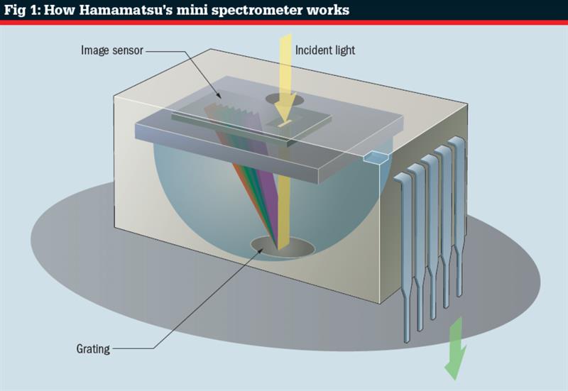
One of Hamamatsu's latest MOEMS offerings is the C12666MA micro spectrometer. This finger tip sized device measures light in the visible spectrum. "A couple of the larger applications for this are colour checking in ink jet printers," Bennett pointed out, "and checking RGB lighting levels on TV and movie sets."
Light entering through a small slit is dispersed into a spectrum by a reflective concave grating created using nano imprinting (see fig 2). The light is then focused on a 256 pixel CMOS linear image sensor. The design allows light of shorter wavelengths to be focused nearer to the entrance slit, with longer wavelengths further away. The sensor then outputs the appropriate signal.
"Hamamatsu has only been offering MOEMS devices for a couple of years," Bennett concluded. "It's still early days and there will be many more devices launched in the next three years or so."


