
With Moore’s Law being pushed to its limits and general-purpose CPUs and GPUs no longer able to meet the requirements of more demanding workloads computing pioneers, John Hennessey and David Patterson have suggested that the industry is on the cusp of a new golden age of computer architecture with the creation of multiple domain-specific architectures (DSAs).
The Open Compute Platform organisation (OCP) has recently seen an explosion of interest in accelerators, with proposals for a wide range of form factors to support accelerators.
Like general-purpose CPUs, DSAs are programmable. Unlike general-purpose CPUs, DSAs also contain a substantial amount of logic tailored to accelerate the execution of specific workloads, resulting in a 5-10X power-performance improvement for their target applications.
Examples include, Google’s Tensorflow accelerator, which contains large internal memories and multiply-accumulate arrays to accelerate machine learning workloads and Netronome’s Network Flow Processor which contains data movement logic and multiple processing threads to accelerate the processing of networking workloads.
While DSAs benefit from being produced on advanced process nodes, at 10 and 7nm nodes, the total cost of silicon product development may exceed $200million and as DSAs serve more focused markets, they may not be economically viable.
Conversely, while DSA development on more mature nodes is cheaper, die sizes may be so large that poor yields make DSA products too expensive.
One solution is chiplet-based product design, which has recently received renewed attention. Here, a product is implemented not as a single monolithic die, but across multiple die in a single package. AMD, Xilinx and Intel have either built or have plans to build chiplet-based products which offer two potential advantages.
Firstly, an accelerator design that requires a large die when implemented as a monolithic product, can be partitioned into multiple smaller die, each of which offers a higher yield. Data from AMD has shown that a large multi-core processor partitioned across four die is 30% more cost effective than the same product implemented as a single die.
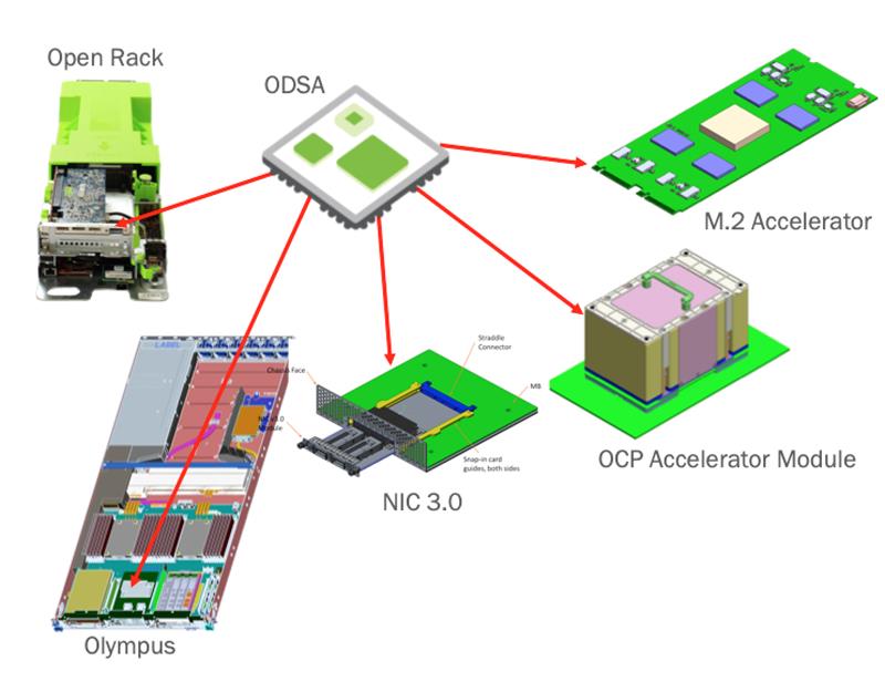
Figure 1: New OCP form factors for accelerators |
Though each accelerator contains domain-specific logic, accelerators of all kinds contain several non-domain specific elements such as general-purpose CPUs, network, memory and host interfaces, internal memory and bus/switching logic. In the Tensorflow accelerator, for example, this domain-independent logic accounts for almost 40% of die area.
Monolithic designs reduce development cost through reuse, by buying 3rd party intellectual property (IP) for these functions. However, IP reuse still incurs significant costs.
Figure 2 shows how DSA products can reuse chiplets instead of IP.
New design effort can be focused on the logic block unique to this new product, reducing development costs.
Secondly, designs composed of chiplets implemented in different process nodes, potentially further reduce costs.
Relative to a monolithic design, chiplets incur both a power and potentially a performance penalty. Data that would be transmitted on-die in a monolithic design is instead transmitted between die. Historically, off-die (and correspondingly off-package) communication has been several orders of magnitude less efficient than on-die communication. Recent advances in short-reach communication and packaging have made inter-chiplet communication achieve efficiency comparable to on-die communication and spurred a renewed interest in chiplets.
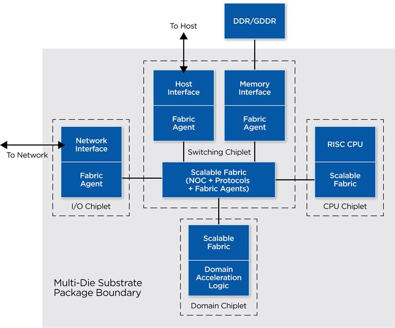
Figure 2: DSA partitioned into and implemented as chiplets |
Open domain-specific architecture
Beyond power-efficient communication, the chiplets in a package have to be functionally integrated i.e. they have to work together as though they are a function implemented on a single die.
This functional integration is implemented with an architectural interface. Almost all chiplet-based products use a closed proprietary architectural interface. Chiplets from multiple companies cannot be easily assembled into an integrated product.
The Open Domain-Specific Architecture (ODSA) project aims to enable the development of domain-specific products that integrate chiplets from multiple companies by developing and implementing an open architectural interface.
The ODSA works to define recommendations and specifications for open interfaces to enable multiple chiplets to work together as though they are a single monolithic die. Figure 3 shows the architectural interface under development. The architectural interface is a memory-semantics based logical interface that is constructed on top of the physical connectivity between chiplets. It allows all the chiplets in a package to share a common address space and allows coherent and non-coherent memory transactions between chiplets.
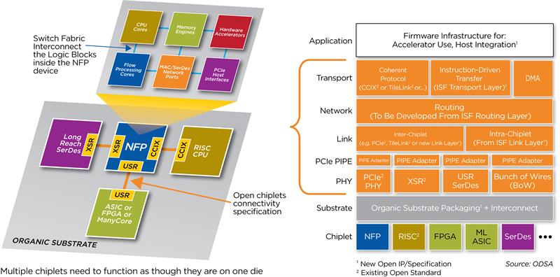
Figure 3: Open interface for chiplet-based design |
This enables software on the chiplets to behave as though the chiplets are a single die.
Finally, the ODSA is also working on common physical descriptions, interface operation, management and test mechanisms.
Chiplet-based products will require a workflow different from that for monolithic designs. For example, one bad die in a multi-chiplet product renders the whole die unusable.
Die will have to be extensively tested before being integrated into a package and being tested as a product - commonly referred to as the known good die problem.
IP normally sold as soft or hard macros will now be sold as die.
Chiplets may in-turn require new types of IP. The ODSA aims to establish good practices to enable the efficient development of chiplet-based products.
The ODSA is also developing reference implementations to inform the development of the architectural interface and business workflow. The first target is a prototype that integrates existing die from multiple companies into a single package.
The second is a PoC that will implement the same functionality as the prototype, but with chiplets that support the new architectural interface. The prototype is a learning platform to identify business and technology issues in developing chiplet-based products – and has already highlighted several issues. For example, bump maps, normally confidential, will have to be shared all the companies building the PoC.
Recent progress
Since its inception in October 2018 the ODSA has grown rapidly. The group produced a white paper with contributions from 10 organisations in December. It runs workshops and in March, the ODSA was adopted as an official OCP project.
Multiple PHY technologies currently exist ranging from the highly parallel interfaces on thousands of low-speed wires to serial interfaces with very few wires, each running at a high speed.
zGlue is evaluating these technologies, including beachfront bandwidth (the length of interface), energy per bit, implementation complexity, portability across process nodes and methods to match technologies to design goals. This is believed to be the first public cross-PHY analysis on common objectives.
Brian Holden from Kandou has proposed a PCIe PIPE abstraction so as to enable a common architectural interface to support multiple PHY layer technologies.
Another proposal from GlobalFoundries and Aquantia is for a new open PHY layer. The proposed interface, derived from the well-known high-bandwidth memory (HBM) interface, can be easily implemented in multiple process nodes.
Quinn Jacobson from Achronix, Jawad Nasrullah from zGlue, Marc Verdiell from Samtec and Larry Zu from Sarcina have developed a design and development plan for the ODSA prototype that targets networking and storage applications.
The ODSA’s objective is to create a marketplace of chiplets from multiple vendors. With these tools, developers can assemble domain-specific architectures to target specific applications at specific power and performance targets by assembling best of breed products from the marketplace.
Author Details: |


