
But flash is dominant despite its properties. In particular, flash has a finite life and data can’t be written and erased by the bit – it uses a page based approach in which blocks are the order of the day. Flash also consumes a lot of power. Even so, demand for flash is growing at 45% per year.
When it comes to integrating flash onto devices such as microcontrollers, the concept brings manufacturing complexity, although that’s not something the industry has shied away from.
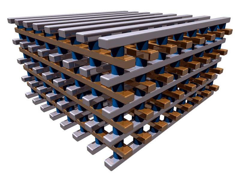
The major challenge to flash comes from Moore’s Law; the smaller the process, the harder it is to make reliable flash memory. With a ‘brick wall’ expected at the 10nm node, manufacturers have started to use a multilayer approach in order to keep flash useable.
Nevertheless, flash memory technology continues to develop – with particular emphasis on the on chip aspect. One of the most recent such developments has been announced by Renesas. It says its one transistor (1T) MONOS flash will bring better performance and reliability to devices aimed at the automotive sector.
Flash, in Renesas’ opinion, has been incompatible with the analogue and power devices used control high voltage drivers for compact motors in automotive applications. This has typically been addressed either by incorporating eFUSE technology or using external EEPROMs.
MONOS, however, isn’t a new technology. Takashi Kono, senior chief professional of the solutions business unit within Renesas’ core technology business division, noted that MONOS technology started out being used in products such as EEPROMs and IC cards. “Renesas has been developing and mass producing non volatile memory using the MONOS structure for more than 30 years,” he said. “The major advantages of the MONOS structure are that it achieves a high reliability by storing charge in traps in the silicon nitride film and that it has high scalability due to its simple structure.”
MONOS differs from mainstream floating gate flash in that it traps charge in a silicon nitride film, rather than in silicon oxide (see Fig 1, main picture). “Since the charge storage layer in floating gate flash is a conductor, if there is a defect in the silicon oxide layers that surround it,” Kono explained, “charge can be lost through that defect, eventually resulting in the loss of all charge.” That isn’t the case with MONOS. “By its very nature,” Kono continued, “MONOS has high reliability in data retention; the most important characteristic for non volatile memory.”
In those 30 years, MONOS has evolved in two directions (see fig 2, below). One such development has been the split gate variant (SG-MONOS). Kono said: “SG-MONOS combines the MONOS structure with a split gate structure – the role of the selection transistor. This technology is used in applications that require high performance and large memory capacities. The split gates are formed from the low voltage, high performance transistors used in the CPU and logic blocks.”
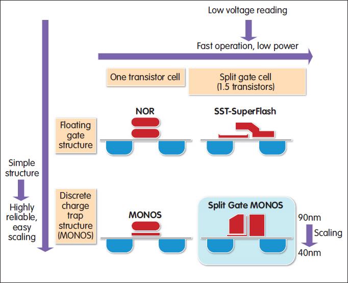 SG-MONOS is not only low power, but can also provide random access to data at rates in excess of 100MHz because the read path is composed of core transistors. A further benefit is that it enables source side injection. The technology lends itself to products that require high performance and larger capacity memories, says Renesas.
“The combination of these features with the inherent MONOS structure means SG-MONOS has large advantages over the conventional floating gate type flash memory widely used in MCUs,” Kono continued. “Renesas uses SG-MONOS as a main technology in its MCUs fabricated in 150nm and later processes.”
The other direction which MONOS has followed is the development of 1T technology. “This can be embedded with a minimal number of additional masks in applications where the percentage of chip area taken up by the flash memory is small,” Kono said. “This technology features a simple 1T memory cell and can be programmed with low power due to tunnelling.”
And it is this technology that Renesas outlined at ISSCC 2016. According to the company, it enables a read/write endurance in excess of 100million cycles at junction temperatures of up to 175°C. It also has a rewrite energy of 0.07mJ per 8kbyte, achieved using adaptable slope pulse control as a means to weaken the electric fields that can degrade memory cells.
“The technology announced at ISSCC 2016just a few additional masks,” said Kono, “whereas ordinary embedded flash requires 10 to 20 more masks. It can also be embedded in a wide range of base processes and can achieve the high temperature reliability required in automotive applications.”
1T-MONOS is said to keep additional process costs as low as possible while providing a way to add flash memory to automotive analogue and power devices. Renesas says this has the potential to reduce the number of chips used in motor control systems, while helping to make them more compact, lightweight and power efficient.
So far, Renesas has developed prototypes of 128kbyte memories using 1T-MONOS technology on a 90nm process. But Kono said the company is planning to start volume production of devices featuring 90nm 1T-MONOS in 2019.
While Renesas has automotive applications firmly in mind when it comes to 1T-MONOS, the company says the technology can also be used to support a range of consumer and industrial applications. As Kono pointed out, the technology is particular suited to those applications where the amount of memory and the area it occupies is relatively small. “Because of this, it can be adopted in products and processes in which flash memory has not previously been embedded.
“These applications,” he concluded, “can now enjoy the benefits of embedded flash. And, since low power program/erase is possible, it will also suit low power applications, including devices being targeted at the IoT.”
While MONOS is looking to provide a better version of flash, other companies are looking to develop alternatives. One in particular is Crossbar, which is backing resistive RAM (RRAM). According to the company, its RRAM technology can outperform NAND flash significantly, offering x1000 faster writes and x1000 the endurance. Along with high temperature operation, Crossbar’s RRAM is said to have more than 40 times the density of DRAM. CEO George Minassian said: “The IoT and wearables markets require energy efficient, secure and low cost microcontrollers. Crossbar’s RRAM technology is an ideal solution to address these requirements by providing embedded memory blocks for program and data storage on chip or as stand alone EEPROM.” Crossbar’s RRAM is compatible with CMOS and is said to scale to small process geometries. This, it contends, will enable the integration of non volatile memory blocks at the same process nodes of MCUs and SoCs. And an indication of its potential comes with the recent signing of a deal with Chinese foundry SMIC to offer Crossbar RRAM blocks on its 40nm CMOS process. |
 Resistive RAM looks to oust flash


