“The goal is to identify, process and characterise these dislocations to fully understand the impact of defects in GaN so we can find specific ways to optimise this material,” says Joseph Kioseoglou, a researcher at the Aristotle University of Thessaloniki.
The researchers used computational analysis via molecular dynamics and density functional theory simulations to determine the structural and electronic properties of a-type basal edge dislocations along the <1-100> direction in GaN. Dislocations along this direction are common in semipolar growth orientations, the team explains.
The study was based on three models with different core configurations. The first consisted of three nitrogen (N) atoms and one gallium (Ga) atom for the Ga polarity; the second had four N atoms and two Ga atoms; the third contained two N atoms and two Ga core-associated atoms. Molecular dynamic calculations were performed using approximately 15,000 atoms for each configuration.
The researchers say they found that the N polarity configurations exhibited more states in the bandgap compared to the Ga polarity ones, with the N polar configurations presenting smaller bandgap values.
“There is a connection between the smaller bandgap values and the great number of states inside them,” said Kioseoglou. “These findings potentially demonstrate the role of nitrogen as a major contributor to dislocation-related effects in GaN-based devices.”
The hope is by understanding more about GaN’s limitations, silicon-based semiconductors performance can be vastly improved.
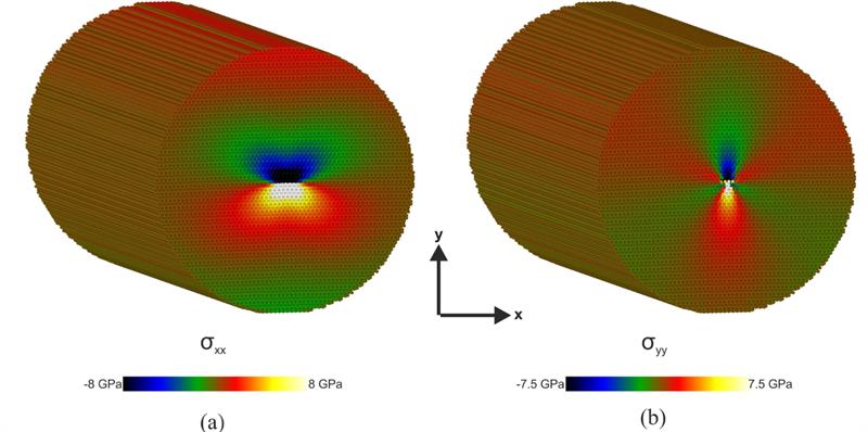
| Distribution of stresses per atom (a) and (b) of a-edge dislocations along the <1-100> direction in wurtzite GaN. CREDIT: Physics Department, Aristotle University of Thessaloniki |