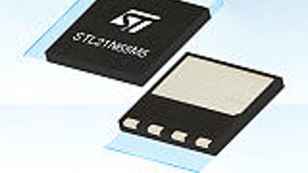
ST announces 'breakthrough' power package
1 min read
STMicroelectronics says it has increased the power density achievable with its latest generation MDmesh V power mosfet technology by introducing an advanced high-performance power package.

According to the power semiconductor specialist, the new 1mm high surface-mount package houses the TO-220 die size within a leadless outline measuring 8 x 8mm and features an exposed metal drain pad for removal of internally generated heat.
ST says its low profile is designed to achieve slimmer power supply enclosures. The new standard is available from ST and Infineon Technologies, which will introduce mosfets using this package. ST's package is named PowerFLAT 8x8 HV and Infineon's is ThinPAK 8x8.
"Our fruitful co-operation with Infineon has produced a high performance package allowing customers to benefit from cutting edge design in a footprint supported by two major global power semiconductor suppliers," said Maurizio Giudice, marketing director, Power Transistor Division, STMicroelectronics. "Our new mosfets combining this package breakthrough with our unique MDmesh V process technology, which is the most advanced in the industry, will deliver the highest power density and efficiency among devices of comparable voltage rating."
Samples of the STL21N65M5 in the PowerFLAT 8x8 HV package are available now with full production scheduled for July 2010.


