
This was achieved by refining the chemical vapor deposition (CVD) growth method by eliminating all carbon impurities inside the copper foils on which the graphene is grown. This uniform, ‘perfect’ single layer, single crystal graphene is expected to find use as an ultrathin support material for high-resolution transmission electron microscopy imaging, and in optical devices.
According to Director Rodney Ruoff’s research group from the Center for Multidimensional Carbon Materials (CMCM) within the Institute for Basic Science (IBS) at the Ulsan National Institute of Science and Technology (UNIST) this achievement differs from the many other thousands of claims made in that none of them had described a truly single layer graphene over large area. Adlayers (bilayer or multilayer regions) have always been present in such films.
IBS scientists refined the chemical vapor deposition (CVD) growth method by eliminating all carbon impurities inside the copper foils on which graphene is grown. CVD on metal foils (especially copper foils) is currently the most promising route for scalable and reproducible synthesis of large-area graphene films of high quality.
The team investigated why “adlayers” appeared in the graphene film grown on copper foils and found that the carbon impurities inside the foil directly lead to the nucleation and growth of adlayers. (Adlayers are regions in the film where there are 2 layers or 3 layers present—multilayer “patches”, that is.)
“We discovered that the commercial copper foils have ‘excess carbon’ particularly near the surface, to a depth of about 300 nm, by using time-of-flight secondary ion mass spectrometry and combustion analysis. From a discussion with one technical expert in Jiangxi Copper Corporation Limited, one of the world’s largest suppliers of copper foils, we learned that the carbon is embedded in the copper foil during manufacture, probably from hydrocarbon-based oil(s) used to lubricate rollers that the copper foil contacts at the high rolling temperatures”, explained Dr. Da Luo, first author of the research. After completely removing this carbon by annealing under H2 at 1060 °C, they were able to achieve adlayer-free and thus truly single layer graphene film.
By applying the same method, the IBS scientists also obtained an adlayer-free single layer and single crystal graphene film on a single crystal Cu foil. One of the first authors Meihui Wang explained, “We thus solved two problems that have persistently been present in prior syntheses of CVD graphene films (adlayers and grain boundaries (GBs)) at one time.”
Having achieved perfect uniformity in the number of layers over a large area (single or double layers, for example) can be used to ensure a consistent device performance. Adlayer regions differ in, e.g., density and size when present in the active regions of devices. In addition to adlayers, GBs are present in polycrystalline graphene films prepared by CVD where graphene islands with different crystallographic orientations join to complete the film. The presence of GBs lowers carrier mobility and thermal conductivity, and reduces the mechanical strength.
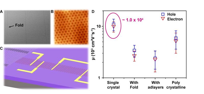
(A) SEM image of an adlayer-free single crystal graphene film with parallel long folds on a Cu(111) foil. (B) A high-resolution ultra-high-vacuum STM image of the honeycomb lattice of the single crystal graphene film. (C) Schematic illustration for straightforward fabrication of high-performance field-effect transistors in the region lying between two adjacent folds in the single crystal graphene film. (D) Carrier mobilities measured from field-effect transistors patterned with various kinds of graphene samples; adlayer-free single crystal graphene film shows the best performance
One feature that raised interest was that it was found that single crystal graphene contains highly oriented parallel “folds” that are centimetres in length, roughly a hundred nanometres in width, and separated by 20 to 50 micrometres. These folds were observed to significantly decrease the carrier mobility of graphene. To eliminate such scattering effects of adlayers, GBs and folds, the team patterned field-effect transistors in the region lying between two adjacent folds and with the transistors parallel to the folds. Unlike folds distributed quasi-randomly in the polycrystalline graphene film, the folds are highly aligned in the large area single crystal graphene film. This makes it easy to fabricate integrated high performance devices from the regions between the folds.


