
The answer to this question lies in a fundamental understanding of the difference between the concepts of resolution and accuracy. Despite being completely different, these two terms are often confused and used interchangeably.
The resolution of an A/D converter is defined as the smallest change in the value of an input signal that changes the value of the digital output by one count. For an ideal A/D converter, the transfer function is a staircase with a step width equal to the resolution. However, with higher resolution systems – 16bit or greater – the transfer function's response will have a larger deviation from the ideal response. This is because the noise contributed by the A/D converter, as well as by the driver circuitry, can eclipse the converter's resolution.
Furthermore, if a DC voltage is applied to the inputs of an ideal A/D converter and multiple conversions are performed, the digital output should always be the same code. In reality, the output codes are distributed over multiple codes (the cluster of red dots seen below), depending on the total system noise,including the voltage reference and the driver circuitry. The more noise in the system, the wider the cluster of data points will be and vice versa. An example is shown in fig 1 for mid scale DC input. This cluster of output points on the A/D converter transfer function is commonly represented as a DC histogram in A/D converter datasheets.
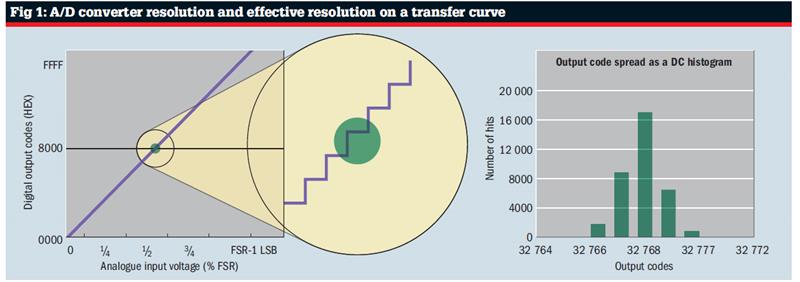
The illustration in fig 1 brings up an interesting question. If the same analogue input can result in multiple digital outputs, then does the definition of A/D converter resolution still hold true? The answer is 'yes' – but only if we consider the quantisation noise of the A/D converter. However, when we account for all the noise and distortion in the signal chain, the effective noise free resolution of the A/D converter is determined by the output code spread – Npp.
noise free resolution = log2(2n/Npp)
where n is the ideal resolution
In typical A/D converter datasheets, the effective number of bits (ENOB) is specified indirectly by the AC parameter and signal to noise and distortion ratio (SINAD), which can be calculated using:
ENOB = (SINAD-1.76) / 6.02
Next, consider if the cluster of output codes – the green cluster in fig 1 – was not centred on the ideal output code and was instead located somewhere else on the A/D converter transfer curve away from the red dot? This distance is an indicator of the data acquisition system's accuracy. Along with the A/D converter, the front end driving circuit, reference and reference buffers are all contributors to the overall system accuracy.
The important point to be noted here is that A/D converter accuracy and resolution are two different parameters and they may not be equal to each other. From a system design perspective, accuracy determines the overall error budgeting of the system, whereas the system software algorithm integrity, control and monitoring capability depend on the resolution.
Having established the differences between the resolution and accuracy for an A/D converter, we now can dig into the factors that contribute toward the converter's total accuracy, often referred to as Total Unadjusted Error (TUE).
Have you ever wondered what 'total' stands for in the TUE specification of an A/D converter? Is it as simple as adding up all the DC error specifications from a datasheet – such as offset voltage, gain error and INL – or is there more to it? As a matter of fact, TUE is a ratio of the total system errors with respect to the operating input range of the converter.
More specifically, TUE is a DC error specification expressed in units of least significant bits (LSBs), which represents the maximum deviation between the actual and the ideal transfer functions of an A/D converter. This specification assumes that no system level calibration is performed.
Conceptually, TUE is the combined effect of the following types of non-idealities in the behaviour of an A/D converter:
- Offset error (VOS). This is the constant difference between the actual and ideal transfer curve of the A/D converter (see fig 2). It is the measured digital output obtained by shorting the A/D converter inputs to GND.
- Gain error. The difference between the actual and ideal slopes of the A/D converter output. It is usually expressed as a ratio of A/D converter range or maximum error at the full scale codes. As shown in fig 2, the absolute value of gain error increases as the analogue input approaches the full scale values.
- Integral non linearity (INL). The maximum non linear deviation of the actual A/D converter transfer curve from the ideal straight-line behaviour. The INL response of the A/D converter has no definite shape and depends on the internal circuit architecture, as well as distortion caused by the front-end signal conditioning circuit.
Most A/D converter datasheets specify the typical and maximum values for all the above DC errors, but not for TUE. Calculating the maximum value of TUE is not as simple as taking the sum of the maximum values of all the individual DC errors. The reason is because all of these errors are uncorrelated and, in the worst case, offset, gain and linearity errors may not all occur at the same input voltage on the A/D converter transfer function. Hence, a simple summation of errors may make the system accuracy look unnecessarily worse. This is especially true if the dynamic range of the application is limited near the middle of the transfer function.
In a typical data acquisition system, there is an input driver and a voltage reference along with the A/D converter and both contribute to the overall offset and gain error. Hence in most systems without calibration, offset and gain errors dominate INL for calculating the maximum value of TUE. A recommended way of calculating the maximum TUE at a particular analogue input voltage is to take the root-sum-square of the maximum values of all individual errors at that point. It is important to convert all of the errors into the same unit, usually LSBs.
TUE=v[|VOS|2 + gain2 + INL2]
This equation typically yields a 'bow tie' shaped error plot. For systems with higher offset error, the 'bow tie' has a thicker knot. However, for systems with higher gain error, the knot of the 'bow tie' becomes thinner and the bows become thicker.
In summary, there is no definitive formula to calculate the maximum value of TUE for an A/D converter because the error is dependent on the input range at which it is being operated. If the system does not require the entire input range of the A/D converter to be used, you can minimise TUE by operating the device away from the end points of its transfer function.
Author profile:
Vinay Agarwal is a systems and applications manager in TI's Precision Analogue SAR A/D converter team.


