
Specifically, device ambient temperature must be kept well below 150°C to keep semiconductor junction leakages low enough not to affect circuit operation adversely. Technology variants, such as silicon on insulator (SoI), can raise the bar by circa 100°C, but most industrial applications require the use of thermal management to ensure the semiconductor junctions remain at a safe working level. In some sectors – aerospace for instance – thermal management is not desired because of the weight penalty imposed by heatsinks and cooling regimes.
Accordingly, alternative semiconductor materials are needed to extend the use of electronics further into harsh environments. Silicon carbide (SiC) is one such material and can be used to create switches, rectifiers and integrated circuits where the low leakage properties can be exploited, making highly integrated circuits feasible at very high temperatures.
To date, though, much of the development focus has been in power electronics and on exploiting SiC’s ability to switch high voltages with low switching and on-state losses and to dissipate internally generated heat.
However, SiC can also be used for small signal electronics – such as analogue and mixed-signal devices – making possible the locating of monitoring and control circuitry much closer to heat sources. Research groups have been exploring various integrated circuit technologies, such as SiC NMOS or JFET based transistors.
Raytheon UK, for instance, has been developing a true CMOS technology with both PMOS and NMOS transistors integrated on the same substrate, interconnected with a refractory metal interconnect system. CMOS in SiC, which Raytheon calls HiTSiC, offers the benefits one would expect from a CMOS process, such as integration density and low current operation.
Electronics which can operate in a high temperature environment is of great appeal in the aerospace industry, for instance, where;
- to improve gas turbine efficiency and combustion control, it will be desirable to make accurate measurements of exhaust gas temperatures with electronics in close proximity to that heat source.
- to reduce electronic noise pick up, sensing electronics can be moved closer to the heat source.
- weight can be saved through a reduction in cabling and heat management hardware.
A number of core small-signal building block integrated circuits already exist as high temperature devices and Raytheon UK’s semiconductors business unit, based in Glenrothes, recently built a thermocouple multiplexer demonstration unit.
|
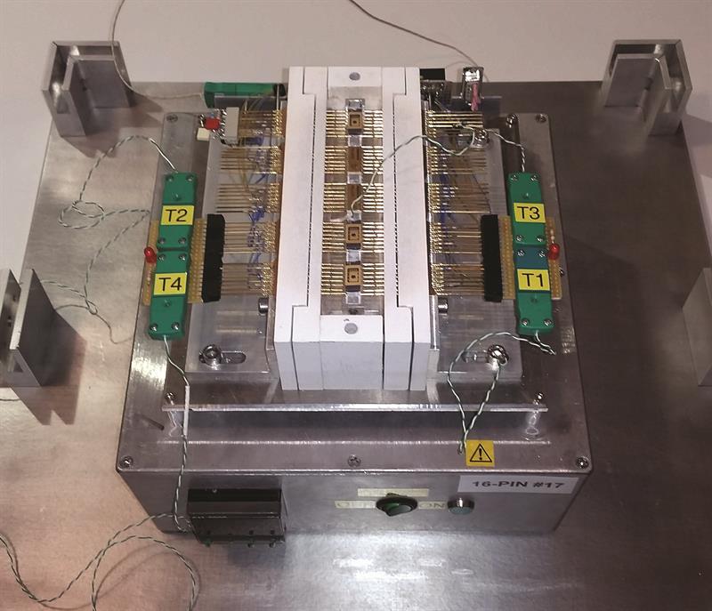 Raytheon’s thermocouple multiplexer demonstration unit has a five chip circuit comprising a 555 timer, two dual D-types providing a counter function and two 4:1 analogue multiplexers. All five chips are SiC-based CMOS devices mounted on a temperature-controlled heated bar and fabricated using Raytheon’s proprietary HiTSiC CMOS process. The devices were gold wire bonded inside 14pin ceramic packages and the pin to pin connectivity (to create the circuit) was achieved using pogo-pins and wire wrap in light of traditional solder’s melting point of 220°C.
Currently, the demonstrator’s mixed signal components have amassed more than 80 hours of operation working at 300°C; with a 4:1 analogue multiplexer benefitting in particular from SiC’s ultra-low leakage property. The device is stable, with an aggregate switch leakage of less than 50nA in the application across temperatures ranging from 23 to 400°C. Also worthy of note is that, in a separate study, HiTSiC digital device performance has amassed more than 1500hr at 300°C.
Though the results are, so far, promising, the industry is some way off having high temperature equivalents of all the Si based devices with which electronics engineers are familiar. Circuits operating at very high temperatures suffer from changes in the semiconductor driven by temperature and time. One particular issue with MOS transistors is the phenomenon of drift in the threshold voltage.
Raytheon UK is working on a Knowledge Transfer Partnership (KTP) project, in conjunction with researchers at Newcastle University, to study the characteristics of the interface between SiC and silicon dioxide – the region which critically impacts on the performance of a MOSFET. The partnership received financial support from the KTP, which aims to help businesses improve their competitiveness and productivity through the better use of knowledge, technology and skills that reside with the UK Knowledge Base. KTPs are supported by Innovate UK, the UK’s innovation agency.
Defects known as ‘traps’ in the SiC-SiO2 interface can fill with electrons during operation and this, in turn, affects the MOSFET threshold voltage value. A detailed understanding of the interface behaviour is enabling Raytheon UK to optimise its SiC CMOS manufacturing processes to minimise the occurrence of traps.
Progress in this field is encouraging, with the stability of HiTSiC NMOS transistors being at least as good as that of any SiC power device available on the open market, but work is continuing to optimise the PMOS transistors. This raises an interesting challenge, since both the NMOS and PMOS transistors are manufactured on the same substrate and the same processing steps are used. However, processing steps optimised for NMOS transistors do not necessarily produce optimum PMOS transistors, and vice versa.
Work is progressing on the development of complementary bipolar transistors integrated along with complementary MOS transistors. This work opens the door to developing precision analogue components which will operate at extremely high temperatures, integrated with conversion and control functions.
Aiming high
The end markets for extreme environment sensors and instrumentation for use in aerospace, oil and gas and geothermal exploration are all set to grow as the technology develops and components capable of high temperature operation become more generally available. SiC-based analogue and mixed-signal devices will certainly have a role to play in serving those markets.
The exploration of HiTSiC technology is not stopping at 300°C, or even 400°C. Research groups are looking at circuit applications which extend operating temperature to more than 500°C – to the point where SiC starts glowing red – and results are emerging where devices survive with good functional operation for tens of hours under these conditions. However, SiC has a theoretical operating temperature of nearly 1000°C.
Although the SiC manufacturing processes are maturing and are producing increasingly stable devices, a variety of packaging and connectivity issues will need to be solved, only some of which were encountered during the development of the thermocouple multiplexer demonstrator.
Author profile:
Ewan Ramsay is a principal engineer with Raytheon UK’s semiconductors business unit.


