
Speaking at the time, Microsoft researcher Doug Burger said: “I would imagine that, a decade hence, it will be common to compile applications into a mix of programmable hardware and programmable software. This is a radical shift that will offer continued performance improvements.”
Steve Mensor, vp of sales with FPGA developer Achronix, noted: “All companies are looking at accelerator technology because data centre infrastructure is getting bogged down through the growth in data and security issues. FPGAs will dominate in applications such as unstructured search and Intel expects 30% of its Xeon processors will have FPGA acceleration integrated in the package or on die in the near future.”
There are a number of reasons why FPGAs are proving attractive as hardware accelerators. “CPUs are sequential,” Mensor pointed out, “They divide functions into smaller parts and their performance doesn’t scale linearly as you add CPUs.
“Hardware accelerators, by contrast, are parallel. They can complete an entire function in a single clock cycle and performance scales as you add accelerators.”
For the moment, the approach taken by Microsoft in Project Catapult and currently being applied by Intel is to use FPGA technology as a coprocessor; either standalone or integrated in a package. Achronix is suggesting that FPGA technology could be integrated into other devices. In Mensor’s opinion: “The concept of FPGA technology being embedded into other devices has been discussed for two decades, but has never been delivered. IBM tried something along these lines in 2000 with Virtex-2 FPGAs; LSI Logic did something before that, but nothing has shipped. The concept of embedded FPGAs is very attractive, but why hasn’t it happened?”
Mensor’s answer is that, in order to embed FPGA technology successfully, developers require FPGA design expertise, as well as IP integration expertise. “In order to be an FPGA expert,” he continued, “you need a lot of customers, because it’s a learning experience every time. IP integration, meanwhile, needs zero risk.”
Achronix believes it has the necessary expertise in both elements and has launched Speedcore; an embedded FPGA (eFPGA) technology. Based on the same architecture deployed in its Speedster 22i FPGAs, Speedcore IP can be integrated into a customer’s SoC.
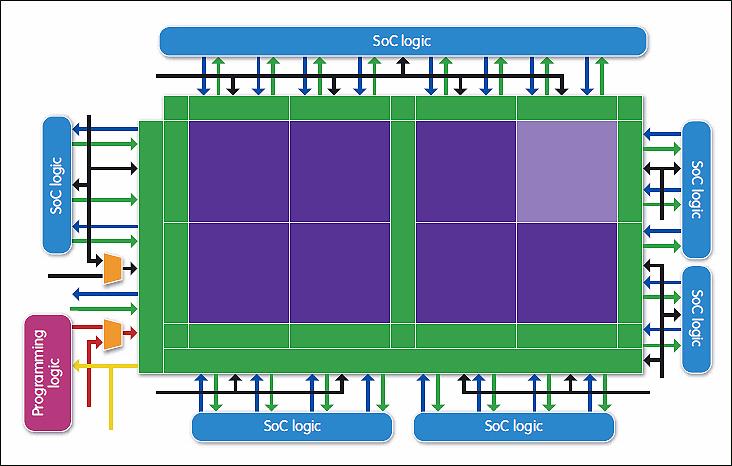
A sample instantiation of an Achronix eFPGA
Mensor noted: “This is the biggest thing that Achronix has announced. The technology is already shipping to customers and we’re getting good feedback.”
Speedcore is said to deliver lower power by offering direct connection to the SoC and by sizing the FPGA element to the customer’s particular requirements. Higher interface performance reduces latency and, because the Speedcore element is smaller than a standalone FPGA, board size and layer count can be reduced. Other benefits are said to include isolation for noise immunity and ESD protection.
The company claims Speedcore could increase data bandwidth by a factor of 10, whilst reducing latency by a similar amount. Mensor added that power consumption could be 50% less, accompanied by a significant reduction in product cost.
One of the reasons why Achronix claims command of both FPGA design and IP integration is because that approach was used to develop its Speedster 22i FPGA. “When we built the 22i,” Mensor explained, “the FPGA logic design was undertaken in Santa Clara, while a team in Bangalore designed the I/O ring. The Bangalore team then integrated the logic core.”
According to Achronix, the Speedster 22i required the integration of SERDES, Ethernet, PCI Express, DDR3, Interlaken and PLL IP from five vendors. “You need to have done it,” Mensor continued. “And Achronix has done its own SoC integration.”
One of the attractions of the Speedcore approach, at least in Mensor’s view, is that it brings power savings. “Both static and dynamic I/O power consumption are reduced significantly,” he said. “And the core static and dynamic power consumption is also lower, because the user can design the core to be exactly the size they need.
“And, if power saving is an important design criterion,” he added, “then the performance can be reduced; you don’t have that ability with a high end FPGA.”

A further benefit is said to be a reduction in the space needed. “High end FPGAs are big,” Mensor observed, “but the FPGA logic only takes up 50% of the die size. Inserting FPGA logic into an SoC means you can build a smaller device.” He added that, alongside area, a smaller device might allow the number of PCB layers to be reduced. “It could require more than 16 layers to route an FPGA,” he suggested, “and signal integrity will also be improved.”
The FPGA logic element can be of any size, Mensor noted. “While there is a minimum size of 8000 look up tables (LUTs), we have customers for Speedcore who are designing cores ranging from 50,000 to 150,000 LUTs. And these have a latency of 2ns, compared to 30 to 50ns in an FPGA.”
Because Speedcore eFPGA is embeddable IP, it does not include programmable I/O; rather, it is intended to be completely surrounded by the end user’s ASIC.
Looking to take some of the challenges out of the FPGA design process, Achronix has developed the Speedcore eFPGA compiler, which is intended to support the rapid development of customer specific IP, along with a modular architecture that allows FPGA cores of different sizes to be created.
Steve Mensor
“There are design rules that dictate the minimum and maximum relative quantities for each of the available resources,” Mensor said, “but our modular architecture allows blocks to be put together in a ‘lego’ like approach.” Amongst the blocks available are: block RAM, with up to 20kbyte per block; logic RAM, up to 4kbyte per block’ a 64bit DSP featuring an 18 x 27 multiplier, a 64bit accumulator and a 27bit pre-adder; and four input LUTs. Additionally, customers can define the Speedcore aspect ratio and the I/O port connections.
“Construction rules are managed in the Speedcore Builder tool,” said Mensor.
While Achronix has a foundry agreement with Intel, giving it the ability to make its Speedster 22i FPGA on a 14nm FinFet process, it will also offer Speedcore in a format ready for manufacture on TSMC’s 16FFT+ process. And, because FinFET transistors age, technology is included to make sure they age uniformly. “We currently have customers designing for the TSMC process,” Mensor noted, “but the customer can choose where they manufacture their SoC.”
Speedcore IP is delivered in GDSII format for the customer to integrate into their ASIC. Achronix also offers ACE design tools that compile designs into the Speedcore eFPGA.
Steve Dodsworth, VP of worldwide sales, concluded: “There is a clear need to have more FPGA integration and this is what Speedcore is all about. Anyone not in the Intel world will be interested in the technology.”


