
To keep up with Moore’s law, the semiconductor industry continues to push the envelope in developing new device architectures containing novel materials. However this, in turn, pushes the need for new solid-state analytical capabilities, whether for materials characterisation or inline metrology.
Aside from basic R&D, these capabilities are established at critical points of the semiconductor device manufacturing line, to measure, for example, the thickness and composition of a thin film, dopant profiles of transistor’s source/drain regions and the nature of defects on a wafer’s surface. This approach is used to reduce “time to data”, which essentially means that we cannot wait until the end of the manufacturing line to know if a device will function as intended, or not.
Every process step costs significant amounts of money and a fully functional device can take months to fabricate.
Analytical techniques
Recent advances in instrumentation and computational power have opened the door to many new, and exciting analytical possibilities.
One interesting example concerns the development of coherent sources. So far, coherent photon sources have been used for probing the atomic and electronic structure of materials, but only within large, dedicated synchrotron radiation facilities. Through recent developments however, table top coherent photon sources have been introduced that could soon see demand in the semiconductor lab/fab environment.
Importantly, the increased computational power, that’s now at our finger tips, is also allowing engineers to make the most of these and other sources through imaging techniques such as ptychography.
Ptychography allows for the complex patterns resulting from coherent electron or photon interaction with a sample to be processed into recognisable images to a resolution close to the sources’ wavelength without the requirement of lenses (lenses tend to introduce aberrations). Potential application areas extend from non-destructive imaging of surface and subsurface structures, to probing chemical reactions at sub femto-second timescales.
Detector developments are also benefiting many of the analytical techniques presently used. A good example of this is transmission electron microscopy (TEM) and scanning transmission electron microscopy (STEM) that can now image, with atomic resolution, heavy as well as light elements.
Combining this with increased computational power, allows for further development of imaging approaches such as tomography, holography, ptychography, differential phase contrast imaging, etc. All of which allow TEM/STEM to not only look at atoms in, for example, 2D materials such as MoS2 in far greater detail, but also opens the possibility to map electric fields and magnetic domains to unprecedented resolution.

Meaningful solutions
The semiconductor industry is evolving at a very rapid pace. Since the beginning of the 21st century, the industry has seen numerous disruptive technologies emerge; technologies that need to serve in an increasingly fragmented applications space and, significantly, it’s no longer solely about ‘the central processing unit (CPU)’.
Other applications, ranging from the Internet of Things to autonomous vehicles and wearable human-electronics interface are being pursued, each of which come with unique requirements and analytical needs.
| “In the long term, the industry will have to think of new characterisation/metrology approaches, with one possible scenario being MEMS based analytical devices” - Paul van der Heide |
In this rapidly changing semiconductor landscape, we, as an industry, are faced with the huge challenge of developing the right supportive infrastructure – with the right analysis facilities that have the right people at the right place, and where meaningful solutions are developed that have valuable impact. And while it’s true to say that we can analyse literally everything, the question that should always be asked is: ‘what is of importance’.
Analysis is costly and many of the major high-volume manufacturing companies do not always have the time to fully explore all the potential areas of interest, and there are many. As a result, the industry is seeing far greater levels of collaboration especially with research institutions such as imec.
Extending capabilities
Looking ten to fifteen years ahead, we can expect to witness a different landscape. Although I’m sure that existing techniques such as TEM/STEM will still be heavily used – probably more so than we realise now (we are already seeing TEM/STEM being extended into the fab).
We will also see developments that will push the boundaries of what is possible.
This could range from the increased use of hybrid metrology (combining results from multiple different analytical techniques and process steps) to the development of new innovative approaches.
To illustrate the latter, take the example of secondary ion mass spectrometry (SIMS) - see the image opposite. With SIMS, an energetic ion beam is directed at the solid sample of interest, causing atoms in the near surface region to leave this surface. A small percentage of them are ionised, and pass through a mass spectrometer which separates the ions from one another according to their mass to charge ratio. When this is done in the dynamic-SIMS mode, a depth profile of the sample’s composition can be derived.
Today, with this technique, we can’t focus the incoming energetic ion beam into a confined volume, i.e. onto a spot that approaches the size of a transistor. At imec however, we were able to introduce novel concepts that resulted in what are called 1.5D SIMS and self-focusing SIMS (SF-SIMS). These approaches are based on the detection of constituents within repeatable array structures, giving averaged and statistically significant information. This way, the spatial resolution limit of SIMS was overcome.
There are also exciting developments occurring here at imec in other analytical fields such as atom probe tomography (APT), photoelectron spectroscopy (PES), Raman spectroscopy, Rutherford back scattering (RBS) and scanning probe microscopy (SPM).
One important milestone has been the development of Fast Fourier Transform-SSRM (FFT-SSRM) that allows users to measure carrier distributions in FinFETs to unparalleled sensitivity. This capability has also been translated into a commercial product which has been installed at several imec partner sites.
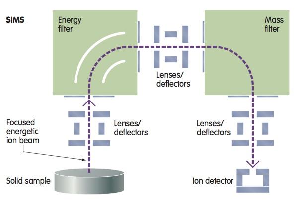
| Above: SIMS uses an energetic ion beam, directed at a solid sample, to provide a profile of its composition |
New analytical approaches?
Much like the rest of the electronics industry, probably, the biggest challenge materials characterisation and inline metrology will face over the next ten to fifteen years will be how to keep costs down.
This will force us to think of totally new approaches and methods. Today, we make use of highly specialised techniques developed on mutually exclusive and costly platforms. But why not make use of micro-electro-mechanical systems (MEMS) that could simultaneously perform analysis in a highly parallel fashion, and perhaps even in situ?
It is quite possible to imagine scenarios in which an army of such units could scan an entire wafer in the fraction of the time it takes now, or alternatively, the incorporation of such units into wafer test structure regions.
In addition, these could be reusable or disposable and if that was achieved, then that would be a true game changer.
It’s a huge challenge, but if it could be done, it would have a significant impact on the semiconductor industry.
| Author details Paul van der Heide is Director of Materials and Component Analysis (MCA) at imec |


