
EnSilica is a leading fabless design house focused on turnkey chip and systems design, with expertise in digital and analogue mixed signal designs. How does it approach selecting the right technology for the design?
David Wheeler, technical director, noted that low power and cost remain drivers. “It’s the same as ever and you could argue that the rise of mobile computing and phones has distorted the market. While a lot of technology supports those markets, there are still a lot of older generation processes. However, the landscape for advanced platforms is following the mobile computing curve.”
Dave Doyle, EnSilica’s sales director, added: “If you’re not on the bleeding edge, want an MCU with control logic, some analogue and sensor interfaces, that lends itself to a mature technology and 90 to 180nm is typical.
“It’s also a cheaper entry point and companies can ‘get into the game’ with a simple mask set probably costing £100k, plus a couple of hundred thousand for NRE. But, on the digital side, it’s going to be 65nm or less.”
FPGAs used to be a popular technology and began to take a central position in PCBs. But is that still the case? Wheeler sees them moving to the higher ground. “They’re now occupying a space in data centres and high performance computing; for example, Amazon has launched a cloud computing platform based on FPGAs. They’re also moving into financial apps and have a role which doesn’t overlap with ASICs.”
He pointed out that some top FPGAs are expensive. “You can pay £1500 and not even get a top of the range part. So they are becoming the device of choice for low volume development platforms, where software teams can get to work before silicon is available.”
As Moore’s Law has moved on, so too has the definition of an SoC. Doyle asked what is meant by an SoC “ASICs used to be seas of gates, while SoCs were standard cell parts. Today,” he argued, “EnSilica views an SoC as something with a processor, probably some mixed signal content and some logic, rather than a purely digital device.”
What has changed is the widespread availability of high performance IP. Doyle noted: “There is much more IP available today than 10 years ago. And there’s more analogue IP, although that’s process dependent.” Doyle also pointed to more connectivity IP, including Ethernet and USB blocks.
According to Wheeler, it’s important to select IP blocks at the start of a project that will reduce the time to market. “If you have an embedded platform and you want networking, you’ll need Ethernet,” he said. “Our approach is to construct a table saying ‘this is who I’m buying IP from’ and work from that onwards.”
One issue with IP is quality; designers often lack confidence that an IP block will do ‘what it says on the tin’. “Verification is a large part of the cost of designing a chip,” Wheeler continued. “The more well verified IP you can use, the better. It’s the same with software; you can use standard libraries. You don’t want to reinvent the wheel.”
Doyle pointed to changes in the cost of IP over the years. “It wasn’t that long ago,” he said, “that you would have been required to pay royalties, as well as a licensing fee. Today, you would be upset if you had to pay royalties.”
And Wheeler agreed. “Attractive licensing models have helped the IP business to take off.”
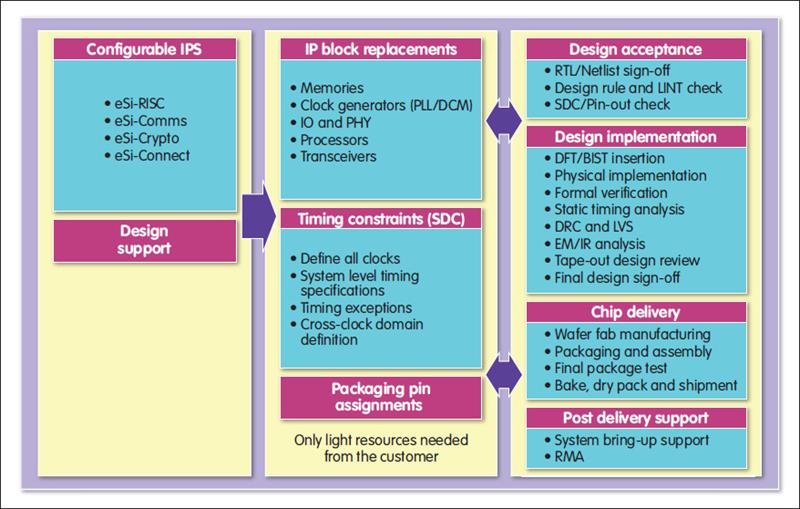 Fig 2: EnSilica and BaySand are providing configurable IP solutions to ASIC UltraShuttle-65 multi-project wafer customers
Volume will also help in selecting the right platform; while a ‘decent’ FPGA is expensive, the entry point for an ASIC design is lower. “We’re happy to give advice,” Wheeler said, “and to understand what is driving the customer. Often, a project will start small, with a second generation device moving to a larger scale. So it’s possible to start with an FPGA, then go to ASIC once the market has developed.
“FPGAs allow you to get to market quickly, with cost savings coming later on with an ASIC – and some customers take that approach.”
Other issues to be considered include the target market. “If it’s automotive,” Wheeler offered, “it might need a particular fab. If it’s military, you can only use certain European fabs.”
Should designers be pre-occupied with process nodes? “If you have a die size that’s acceptable for good volume on an older process, there’s no point in going to a smaller node, unless it’s to reduce power or area,” Wheeler said.
While EnSilica designs at nodes across the board, its customers generally have medium volume requirements. “That’s around 1million,” Wheeler said, “and the sweet spot for this is often 22nm. But older nodes have better yields and you can get a 99% yield from them.”
When it comes to mixed signal designs, Doyle said there are usually two categories. “Either companies are trying to hit power/cost targets by reducing the number of discretes or they have an idea, but don’t know how to implement it.
“In the first case, it will be cheaper than a discrete based design, no matter what geometry, so start large. Those who have an idea will generally know a price point – and that will lead to a particular process.
“In the end,” he said, “it’s what will meet the specs and what’s the cheapest way to do it. And we find mature technologies serve people well.”
Wheeler pointed out that software will always come into the equation at some point. “Do you need an 8051 or a 32bit processor? Do you need a cache and will this be on or off chip? DRAM or flash? How big is the program code? Can it be held on chip? There’s a lot to be considered outside of the hardware domain, but those things impact your hardware technology choices.”
And there’s the issue of what packaging to use. “It’s a question which is up there in early discussions,” Doyle noted. “What’s interesting is there seems to be a disconnect between chip designers and board designers. We talk to companies who need a low price for their design and are looking at flip chip packaging until we ask about their board manufacturer’s track and gap capabilities. Flip chip might mean they need an eight layer board, instead of four, so they go back into a thin plastic package.
“That’s before you get into other questions like reliability and environment factors,” he continued. “Packaging is a significant part of our overall discussion and has a huge bearing on final price.”
So is the advanced platforms landscape changing? “Dramatically,” Doyle said. “Three years ago, EnSilica had a good mix of designs; today, there’s not much FPGA work and 50% of our work is ASIC services, with 20% IP and 30% mixed signal SoCs.
“Looking forward,” he concluded,”it will change even more. ASIC will be 25% and IP 20%, with mixed signal SoC design and supply chain management taking the lion’s share.”


