
5G is intended to offer data rates in excess of 10GBps, extremely low latency, and uniform coverage over a wide area, as well as a thousand-fold increase in capacity. It is expected to enable and encourage the development of new markets, technologies and applications beyond high-speed mobile communications, including massive machine-type communications (mMTC) – the enabling technology for the cellular constituent of the IoT – as well as mission-critical applications (such as autonomous vehicles), and even last-mile fixed broadband.
Because of the high target data rates for 5G, large chunks of contiguous spectrum will often be required, and as a result mmWave is considered to be a key component in the roll-out of 5G.
Until recently, the mmWave bands above 24GHz that are under consideration were considered inappropriate for mobile and non-line-of-sight use. However, research has now shown that those issues can be addressed and overcome. Utilising these bands will be a key factor in the new 5G radio interface.
While the specific frequency bands are yet to be finalised, as an independent design house working with many of the key industry players Plextek RFI has been able to form a picture of the bands where most current design activity is taking place. The likely operating frequencies include the nominal 28GHz (27.5 - 28.35GHz), 37GHz (37 - 38.6GHz) and 39GHz (38.6 - 40GHz) bands, all of which are already licensed by the FCC in the USA.
In Europe, the Radio Spectrum Policy Group (RSPG) launched a strategic roadmap for 5G in November 2016 in which, in addition to specifying new and existing sub-6GHz bands, it recommended the 26GHz band (24.25 to 27.5GHz) for the high-bandwidth spectrum that will be needed to provide ultra-high capacity. In the UK Ofcom has said it wants to promote this as the ‘pioneer’ band for 5G in Europe and as the priority band for global harmonisation. Bands centred at 32GHz and 42GHz have also been highlighted as longer-term options.
Device process technology
Most mmWave 5G systems will be based on phased-array or switched beam antenna architectures, and many design houses are currently involved in designing custom MMICs for such prototype systems. Key components required for the mmWave front-end include power amplifiers (PA), low-noise amplifiers (LNA), phase shifters and switches. GaAs pHEMT processes are an attractive option for PAs, as they offer adequate RF power output, high linearity and high power added efficiency (PAE) at a modest supply voltage. GaN, which is growing in popularity for many applications, is another contender that offers higher power density but has the disadvantage of requiring a higher supply voltage. GaAs pHEMT is also seen as a good option for LNAs due to its superior noise figure performance, although in the longer term LNA may be integrated into a transceiver, when SiGe or even CMOS or silicon-on-insulator (SoI) would be the likely technology choice. For upconverters and downconverters Plextek RFI is, for example, working on pHEMT solutions but other companies are using SiGe, CMOSand SoI.
For RF switches, the main technology options are PIN, pHEMT and SoI, with PIN proving to be the best for low insertion loss and high power handling at the higher frequencies. Plextek RFI recently designed a 28GHz Single Pole 4 Throw (SP4T) switch chip suitable for 5G, which was realised on a newly-released PIN diode IC process from WIN Semiconductors.
Packaging options
The packaging of mmWave ICs can present some significant challenges, since at these high frequencies even short bond wires have appreciable inductive parasitics. In addition the parasitics of the package and the PCB on which it is to be mounted must be considered. However, with careful design and attention to detail there are several SMT packaging options that can be used to provide good performance.
Over-moulded plastic packages, where the device is assembled onto a leadframe and covered with plastic, are typically usable up to about 30 to 40GHz depending on the functionality of the IC. At Plextek RFI we have used air-cavity plastic packages, which are similar to over-moulded but have an air-filled cavity above the device, up to 42GHz. In both these cases a custom leadframe is often used to optimise performance. Laminate packages are normally custom-designed for higher frequencies and – because they allow the chip surface to sit at the same level as the package – permit the use of shorter bond wires and can work up to about 45GHz. We have designed a custom laminate package for a customer’s own 39GHz switch IC for 5G, many thousands of which have already been shipped – even before the 5G standards have been defined.
mm-wave 5G Components
Figure 1 includes a shot of a 39GHz GaAs PA chip processed in a commercial GaAs foundry, packaged by a volume manufacturer in an air-cavity plastic package with a custom leadframe and mounted on a PCB for evaluation in a representative end-use environment. The output of the chip shows an array of transistors that are power-combined to achieve the required RF output power level while still providing adequate gain. There are four stages of amplification, and an integral power detector at the output.
The output third order intermodulation (OIP3) of this IC is shown in Figure 2, demonstrating excellent linearity with an OIP3 of +40dBm across the full 37 – 42GHz band.
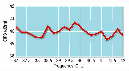
Figure 2: The chip's OIP3 demonstrates good linearity
Since the recent announcement of the 26GHz pioneer band, Plextek RFI has designed a dual-band PA that works in both the 26GHz and 32GHz bands. Because it looks likely that 5G mmWave spectrum allocations will vary between countries, it is almost certain that multi-band components will eventually be required for high-volume mobile terminals. The chip photo (inset) in Figure 1shows four RF amplifying transistors in combination at the output. Other transistors situated around the chip perform switching operations between the two bands, although at these frequencies FETs act more as variable reactances rather than conventional switches.
Figure 3 shows the power output at 1dB compression and the power added efficiency (PAE) at the 1dB compression point for each of the two bands of operation. The power output is approximately 1W in each of the bands. There is some trade-off in PAE for the dual-band design, but the 27 – 30% figures being achieved are still acceptable. For components to be used in mobile devices, cost-effectiveness is a major consideration, and this design meets that criterion.
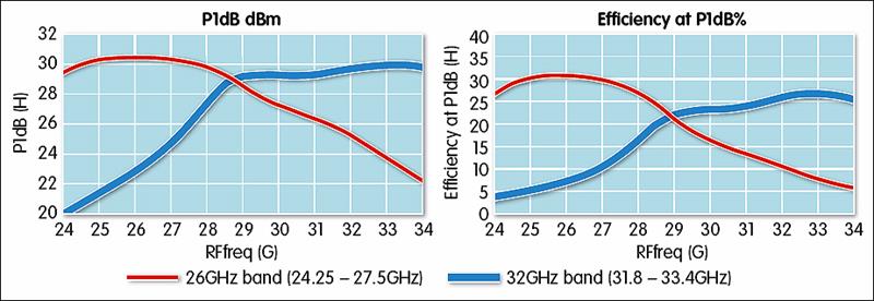
Figure 3: The power output at 1dB compresison and the power added efficiency at the 1dB compression point for each of the two bands of operation
Conclusion
Manufacturers are currently pouring massive resources into developing the components that will enable 5G. Innovative design and packaging solutions are likely to emerge, but those described here are among the leading contenders. In the longer term, it is considered that dual-band and multi-band components are highly likely to be required because of the different mmWave spectrum allocations that are being announced around the world.
Author profile
Liam Devlin is CEO at Plextek RFI.


