
Here's one statistic that highlights that complexity and one that might come as a surprise. A 100mm2 SoC with 10 layers manufactured on a leading edge process can feature up to 1billion transistors. Those transistors and layers may be linked by some 10bn vias. Even more surprising, perhaps, is the fact that all those copper interconnections, when placed end to end, will stretch for something like 20km.
Sree Kesapragada, global product manager for metal deposition with leading equipment manufacturer Applied Materials, said: "There are more and more transistors, more and more interconnects and interconnect technology is facing a critical roadblock."
Creating those interconnects is the challenge. "They are made in situ," Kesapragada noted. "Making that typical SoC will probably require between 80 and 100 process steps, grouped into three segments: lithography, the exposure of a pattern; patterning, the selective removal of material to create wiring pathways; and metallisation, the creation of the interconnecting copper wires. Interconnects, as a result, are very narrow and packed together very tightly – they may only be separated by a few hundred atoms. Patterning therefore plays a key role in their creation."
Building this typical SoC is much the same as trying to fit a quart into a pint pot. "Complexity is one of the challenges," Kesapragada continued. "There may be 1bn transistors, but no two interconnects can interact. Designers quickly run out of real estate and need to employ multiple levels of wiring.
"Meanwhile, process scaling is resulting in vias that may only be 20nm wide."
When dimensions decrease to that level, alignment becomes paramount. "It's a challenge because vias are created one level at a time, so alignment has to be accurate," Kesapragada observed. "With a 20nm via, it's likely that the alignment tolerance is going to be 1nm or less." When alignment falls out of tolerance, manufacturers will see increasing yield issues.
"Compressive stress of the TiN hard mask can distort everything and make metallisation impossible." - Sree Kesapragada |

Hard mask technology is a solution to this problem. "Fabs have a process flow which makes the interconnects less sensitive to alignment error. The process, called metal hard mask, ensures the alignment remains in spec," Kesapragada said.
With metal hard mask, a layer of titanium nitride (TiN) is laid down which matches the interconnects required for that particular step of the process. Because TiN is very hard, it ensures the dimensions of the etched vertical and horizontal interconnects meets requirements. "TiN is one of the hardest materials known to us," Kesapragada pointed out. "It's key to the robustness of the process."
According to Applied Materials, the TiN hard mask film is essential for pattern fidelity and has been used in semiconductor production since the 90nm node.
But despite its applicability to the problem, TiN hard mask technology has its issues. Amongst these are film density and stress. If film density is too low, the hard mask can be eroded during the etch process and the critical dimension of the via could move out of spec, potentially allowing shorts between neighbouring interconnects. Meanwhile, if stress in the hard mask film is too high, the dense patterns laid down during the lithography process will buckle. "Compressive stress is acceptable," Kesapragada noted, "when you are dealing with patterns with large dimensions. However, as these dimensions get smaller, compressive stress of the TiN hard mask can distort everything and make metallisation impossible. And this is going to be a growing problem as designs move beyond the 20nm node."
A further trade off in this process is the porosity of the dielectric; the more air, the lower the dielectric's capacitance. However, when there's more air in the dielectric, it becomes more likely to buckle beneath the compressive stress of the overlying TiN mask. If that stress is reduced, it tends to reduce film density and create more etch problems.
"Hard mask technology for the 10nm node and beyond needs tensile stress and high film density," Kesapragada highlighted. "While physical vapour deposition (PVD) is the leading technology for metal deposition, conventional systems won't accomplish this, so it needs a breakthrough."
And Applied Materials believes it has created that breakthrough with the launch of Endura Cirrus HTX, said by the company to be the first system to allow the tensile deposition of high density films.
Applied's PVD technology enables titanium atoms to be sputtered reactively in a nitrogen based plasma. It adds the system allows tuneable composition.
|
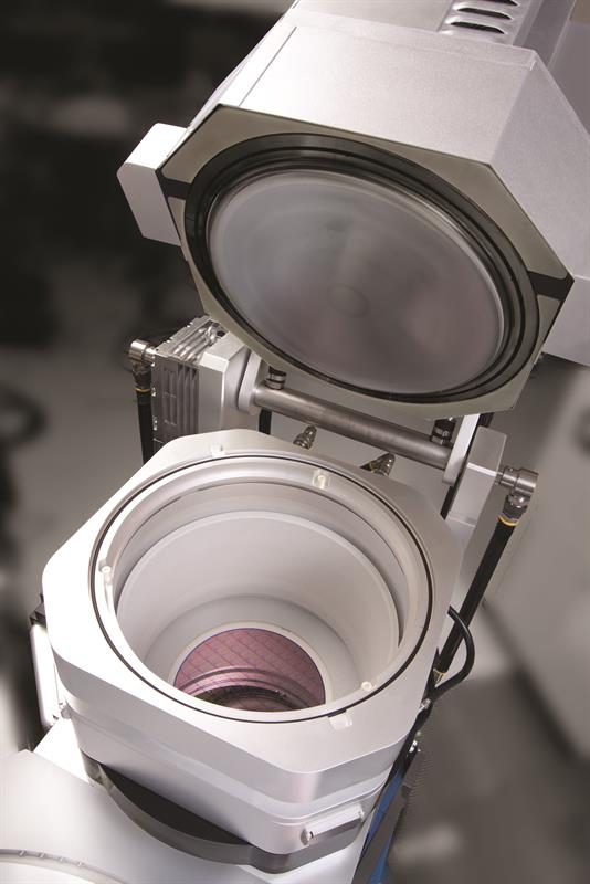 Endura Cirrus HTX is said to be the first system to allow the tensile deposition of high desity films
The PVD technology has been available since 2007, since when more than 200 systems have been installed. Along the way, the technology has been upgraded, with the addition of ionised PVD and energy control, along with higher temperature operation.
The latest update – Cirrus HTX – makes VHF based PVD available to manufacturers. "It has been in development for the last two years," said Kesapragada, "and we have been engaged with memory and logic foundries."
He said the key to Cirrus HTX is to ionise all sputtered atoms. "But ionisation is one thing," he continued, "manipulating those ionised atoms is another. If you can control the ion energy, you can then grow the film in the way you want."
The approach also aligns atoms on the wafer and provides them with enough energy to allow them to be moved around and to create a dense film.
The success, or otherwise, of the process is down to nucleation: how the ions 'stack up' on the wafer. With a neutral dominant plasma, the TiN film will have a columnar structure dominated by the so called (111) orientation. However, with the highly ionised approach of Cirrus HTX, the film develops as a smooth dense microstructure dominated by the (200) orientation. "In this way," Kesapragada commented, "it is now possible to build tuneable films."
The resulting TiN film is said to achieve an ideal combination of tensile stress and high density. This, in turn, brings better etch selectivity, critical dimension line width control and via overlay alignment, as well as better fidelity of dense complex patterns. The company says that film thickness uniformity and low defectivity will minimise variability and produce precise patterning.
Kesapragada concluded: "This approach is already being used in volume production at the 20nm node and will work at 10nm – maybe 7nm – on 300mm wafers."


