
The 112G LR SerDes PHY is seen as a great option for engineers; delivering optimal performance and flexibility to even the most challenging systems. When it comes to looking at implementing 112-gigabit-per-second (Gbps) analogue-to-digital converter (ADC)-based long-reach (LR) SerDes PHY (112 LR SerDesPhy), there are a number of considerations designers will need to keep in mind.
For starters, they will need to revisit Shannon’s equation, which relates to a system’s SNR to the maximum BER that can be achieved.
In summary, the equation states that channel capacity (C) is equal to channel bandwidth (B) that’s measured in Hertz times Log in the base two of the quantity 1 plus SNR. The channel data rate is proportional to the bandwidth and the log of SNR in base two.

Figure 1: The Shannon equation (above) relates system SNR to maximum BER that can be achieved
Therefore, the SNR is significant for how the BER is achieved. The bandwidth is usually Nyquist, which is 28 gigahertz (GHz) in the case of the 112G LR SerDes PHY. In this case, bandwidth is not an option for design purposes. The Nyquist bandwidth is set by the standard to be 28 GHz and is set by the channel.
SNR is available as an option and can be used for workarounds. SNR must be a certain number set by the error rate of the link. For example, it can be shown that for a PAM-4 link with Gaussian noise, achieving 1E-12 BER, the SNR has to be 24.5 decibels (dB). But what does this 24.5db SNR really mean? First, the signal derives from a PAM-4 transmitter that reliably sends symbols over the line. The noise is a result of the receiver, which has a number of components.
In theory, by increasing transmit signal amplitude, the SNR can be increased to improve BER. There is a limit to the transmitting amplitude set by the IEEE specifications which limits the options on transmit side.
There is considerably more innovation at large with SNR on the receiving side. However, engineers will need to consider the certain losses involved as data travels from the PAM-4 transmitter to the receiver on the far end.
For example, signal loss due to skin effect, dielectric loss, crosstalk, device noise, ADC quantisation noise, and jitter. Forward error correction (FEC) will, however, mitigate the overall SNR requirement.
Signal loss caused by skin effect increases the loss of the conductor, since only the outside of the conductor is used. Dielectric loss refers to heating up the cable. These two losses combined reduce the signal at the receiver’s input. Therefore, you will end up with a reduced SNR due to the amplitude because of the signal losses.
Another component that reduces SNR is crosstalk. For system designs using the 112G LR SerDes PHY, we usually have an SNR budget, it’s called a “link budget” that needs to be at least 24.5dB for example. Therefore, crosstalk needs to be accounted for in this budget, along with other noises in the system including device noise and jitter.
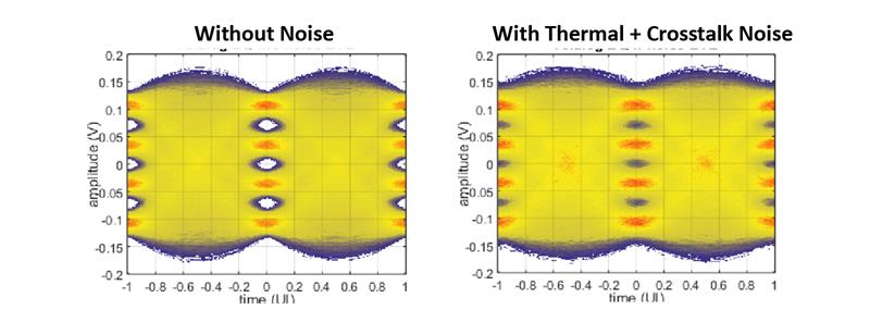
Figure 2: On the left, the eye diagram without noise. Just the opposite on the right eye diagram which is closed
Take device noise for example. When a transistor amplifier is operating and processing a signal, it’ll take a weak input signal to make it bigger.
However, when it amplifies a signal it also adds noise, because all active devices including transistors will bring noise to the signal that they are processing. Therefore, designers must consider a device noise budget.
Up next is jitter referring to random variations in the ADC sampling clock in the 112G LR SerDes PHY. This phase noise also raises the noise-floor of the system. Therefore, to achieve the desired BER there must be noise allocations within the budget for crosstalk, offsets, device noise and jitter.
Additionally, when we look at the ADC-based 112G LR SerDes PHY, SoC and system designers have extra considerations, as they must also contend with analogue-to-digital converter (ADC) quantisation noise, another factor that reduces SNR. Therefore, the budget for this specification needs to include an allocation for all of the above losses and noise sources, as well as quantisation noise.
What about FEC?
The FEC is a coding technique used to transmit data faster than required. Data is transmitted with some overhead which is used to correct errors in the data stream as a way to mitigate or increase the system’s SNR margin. The margin is defined as the SNR in dB beyond the minimum requirements. A SoC or data centre system designer can have zero channel operating margin (COM).
Or, if one were to add FEC to the link, they can easily achieve an extra 6 or 7dB, which gets the margin back. The cost of FEC includes the overhead, the power and area of the FEC circuit blocks, and latency, which is the delay required to encode the transmit and decode the receive data.
If the data centre system designer opts not to use a FEC, or if a particular vendor doesn’t include a FEC in its PHY, that system designer would have to reduce cross-talk or alter the 112G LR SerDes PHY design in order to put that margin in.
SNR is allocated into signal loss, crosstalk, device noise, jitter and quantisation noise. FEC improves the SNR by adding overhead and delay to the data link. Combined, they must add up to a number that is greater in SNR than the minimum required. That extra margin is known as channel operating margin or COM, which is vital in the 112G LR SerDes PHY.
Challenges of 35dB Losses
Figure 2 shows two eye diagrams. On the left, the eye diagram is without noise. It represents standard impairments in the channel, but it shows that the eye is open; all contours and colour differences are smooth and organic. It is just the opposite with the eye diagram on the right, which is closed. But it’s closed in such a way that it’s smooth, although the difference it’s showing is due to device noise, jitter and crosstalk. These impairments reduce the link margin.
Figure 3 shows two simulated eye diagrams showing PAM-4 in the digital signal processor (DSP) of the 112G LR SerDes PHY and represent an example of quantisation noise. The diagram on the left employs an 8-bit ADC. Shown is the output of the DSP (Digital Signal Processing). The eye at the right is open and appears fairly smooth. On closer inspection, there appear to be jagged edges on it and some discontinuities, which are normal. However, it has the characteristics of a good eye at the DSP output.
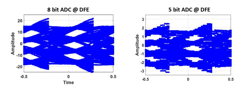
Figure 3: Two simulated eye diagrams showing PAM-4 in DSP and represent a quantisation noise example. The left diagram employs an 8-bit ADC. On the right, the eye diagram is simulated with same condition, but a 5-bit ADC is used
On the bottom, there is another eye diagram simulated with the same conditions. However, the SoC designer used a 5-bit ADC in the simulation. At the output of the DSP, the eye diagram appears cloudy and not very symmetric. It’s small and granular showing the effects of quantisation noise.
Quantisation noise is different than continuous noise because it’s statistically different from other sources. The quantisation noise probability density function is often modelled as a uniformly distributed random variable. Both Gaussian and uniform types of noise need to be accounted for in the link margin. To reduce quantisation noise, for example, the SoC/system designer adds more bits to the ADC or similarly the data path from the ADC through the DSP.
Each time a bit is added to the ADC of a 112G LR SerDes PHY, quantisation noise is cut in half, improving the COM.
Improving quantisation noise gives a smoother eye, however that doesn’t help with the device and crosstalk noise. Adding a bit to the ADC addresses the part of the noise budget related to quantisation noise. Adding more bits to the ADC increases area and power, as well as complexity to the circuit block in addition to increasing the data path size through the DSP. The DSP cannot take advantage of more ADC bits unless it is designed appropriately. Also, the DSP needs to be designed such that we minimise the accumulation of arithmetic noise due to round-off.
Channel operating margin
Quantisation and device noise, crosstalk, jitter, and DSP arithmetic noise – all need to be considered together and then margin added on top to assure a reliable channel operating margin (COM). Optimal solutions balance out the cost mitigation of these noise effects. For example, continuous time linear equalisation (CTLE) can be improved to reduce device noise giving an improvement similar to or a bit added to the ADC. DC Offset cancellation and gain-control circuits can better use the dynamic range of the ADC, reducing its required resolution.
The 112G LR SerDes PHY suppliers, like Rambus, take a detailed, system-level approach. In this case, different noise sources are accurately modelled and simulated at the top level. Those different noises are traded off each other all the while focusing on the link margin. The objective here is to arrive at a reliable link with the best overall cost. However, solutions can differ depending on the amount of equalisation and type of FEC needed.
Why 112G LR SerDes PHY?
The aim is to offer 112G LR SerDes PHY that operates seamlessly over challenging long reach signalling data centre environments. To achieve the greatest product with lowest cost, it is vital that all of the different noises are effectively balanced.
With regards to this, SoC and data centre system designers should be wary of a 112G SerDes LR PHY receiver with a higher power than usual, but with the same operating margin. As previously mentioned, the channel operating margin is the remaining SNR required beyond the Shannon equation limit. No one designs a system without any margin, so that SNR is the bare minimum. Margin is always added on top of that and has to be done so in such a way that the link has competitive area and power.
Author details:
Shaishav Desai is Sr. Director Engineering at Rambus


