An electrically noisy environment, such as within automobiles, is a big challenge for data communication links. Although a CANbus link, combined with isolation, can provide sufficient noise-rejection, it is a complex, costly solution. For this reason, Linear Technology developed isoSPI, a two-wire adaptation of the standard Serial Peripheral Interface (SPI).
The isoSPI interface translates a full-duplex SPI signal of up to 1Mbit/s into a differential signal, which is then transmitted via twisted pair and a simple, inexpensive transformer. This interface is integrated into Linear Technology’s most recent battery stack monitors, a set of analogue integrated circuits designed to measure battery stack cell voltages. There are two isoSPI ports in the LTC 6811, a 12 cell battery monitoring IC. These ports enable multiple LTC6811 devices to be daisy-chained for monitoring long, high voltage battery strings. With isoSPI, modules containing a subset of battery cells can communicate over long distances to one master processor.
How isoSPI works
The isoSPI interface uses differential signalling on a ‘balanced’ pair of wires, where neither wire is grounded. With this configuration, the ‘common mode’ noise imparted onto the wires by external EMI is nearly identical on both wires; the transmitted difference-mode information signal remains unaffected. The isoSPI interface uses a transformer to magnetically couple and electrically isolate this signal between devices. This shields each device from common-mode voltage swings created by system noise while transmitting the important difference information across the dielectric barrier. This is the same technique used in the Ethernet twisted-pair standards.
Furthermore, electrical isolation allows packs to be interconnected despite large DC voltage differences between them. The transformer is selected for the appropriate DC stand-off voltage. Figure 1 shows an idealised isoSPI differential waveform; the DC-free pulse signal is then transformer coupled without information loss. The width, polarity, and timing of the pulses encode the various state changes of the conventional SPI signals.
These isoSPI characteristics were selected to ensure error-free transmission while subjected to the rigours of bulk current injection (BCI) interference testing. In practice, performance against a 200mA BCI has been demonstrated and duplicated at key automotive companies, qualifying isoSPI links for chassis-harness vehicle wiring. This is a key requirement if inter-module communication is necessary and, since electrical isolation is required for safety, isoSPI provides cost savings.
Reducing complexity
A BMS can be designed by connecting battery cells to an analogue front end (AFE) device, such as the LTC6811. Multiple AFEs can be interconnected and connected to a central processor via a CANbus link. Figure 2a shows a structure with two AFEs that support conventional SPI data connections. To achieve the galvanic isolation required for safety and data integrity, dedicated data isolators are required for each AFE. To isolate each cell-stack from the host microprocessor and the CANbus network, galvanic isolation can be provided with magnetic, capacitive, or optical means. When using SPI, isolation is required on each of the four SPI signals.
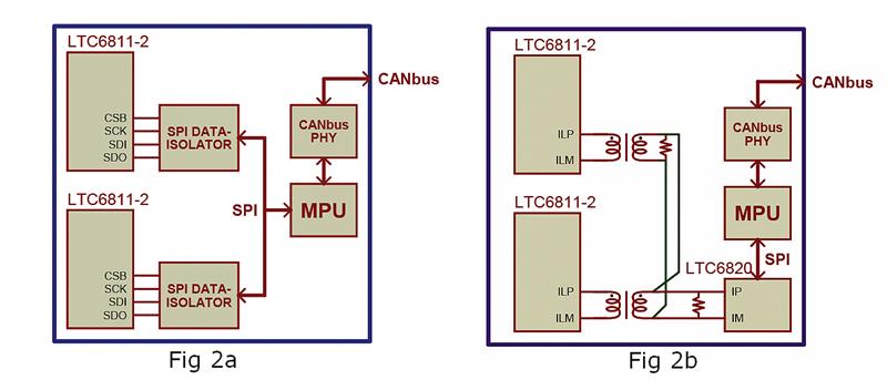
Figure 2. Conventional BMS Isolation vs. isoSPI Method
Figure 2b shows the same functionality, but implemented with isoSPI. A transformer replaces the data isolator to provide the galvanic barrier between the host processor elements and the battery pack potential. At the host microprocessor, a small adaptor IC provides the isoSPI master interface. The A/D converter units shown include integrated isoSPI slave support, so the only additional circuitry required is proper passive termination components that a balanced transmission-line structure requires. While Figure 2 shows two AFEs, up to 16 can be serviced on a single extended isoSPI bus.
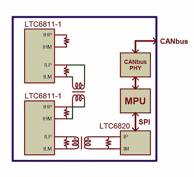
Figure 3. Popular BMS configuration with isoSPI daisy chain
Multidrop or daisy-chain
The isoSPI links will work with simple point-to-point connections and, as shown in Figure 3, dual-port A/D converters to form fully isolated daisy-chain structures. There is a similar overall structural complexity involved in either the bus or daisy-chain approach, so particular aspects of a design may favour one or the other, depending on the subtleties involved.
The daisy chain tends to be less expensive, since it generally involves simpler transformers with a lower DC standoff voltage; transformers for the addressable topology must span the full voltage from the isoSPI master to the AFE, which can be at the top of the full battery stack. On the other hand, the parallel addressable bus has better fault-tolerance since communication is direct to the isoSPI Master. To avoid multiple points of EMI ingress and issues with multipath reflections, bus structures are best kept to single-board implementations so that the bus itself is compact and possibly protected by PCB ground-planes.
Partitioning the BMS electronics
One of the benefits of isoSPI is its ability to operate with lengthy exposed wiring in point-to-point and daisy-chained configurations. Prior to implementation of isoSPI, the BMS design was constrained to a centralised architecture or to implementing an expensive isolated CANbus for interconnection. The isoSPI interface has enabled a practical modular approach with all of its associated benefits.Figure 4 shows a distributed daisy chain BMS structure that allows the pack to be arbitrarily modular and function as a distributed network. The network may have as many AFEs (LTC6811-1) and harness-level interconnects as needed to satisfy the distribution of circuitry.
The use of isoSPI networking means that all data processing activity can be consolidated into one microprocessor circuit, and the microprocessor can be placed practically anywhere. This flexibility allows an isoSPI-based BMS system to be designed for both high-performance and cost-effectiveness.
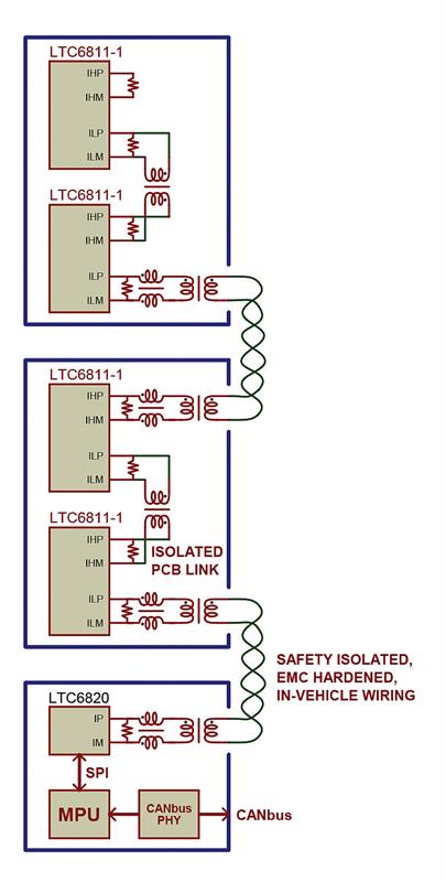
Figure 4. Flexible distributed BMS structures with isoSPI
Note in Figure 4, wherever an isoSPI segment is exposed to harness-level EMC conditions, a common-mode-choke (CMC) is placed in the termination structure of each AFE IC. The CMC is a transformer element that completes the rejection of any residual very high frequency common-mode noise that may leak through the inter-winding capacitance of the coupling transformer. Additionally, all harness wiring is fully isolated for complete safety.
Meeting new challenges
Since the isoSPI structure minimises the amount of electronics resident within cell modules, new directives like ISO 26262 are more easily and cost-effectively addressed. Take redundancy aspects for example; one can simply add extra copies of the AFE sections and add them to the isoSPI network as needed.Also, with the consolidated processor functionality afforded by the networking approach, providing redundant data paths and even dual processors without major packaging impact is simple; add additional circuitry in the various modules as needed to achieve the reliability targets.
By integrating tried-and-true data communication techniques, isoSPI provides a means of remotely controlling standard SPI devices that formerly required an extra protocol adaptation to CAN bus. The isoSPI two-wire data link is a cost effective way to improve the reliability and structural optimisation of BMS through flexible networking of the A/D controllers. Consolidation of the processor function away from the cells enables simplification of pack modules, thus minimising the per-cell electronics content.
Author profile:
Jon Munson is a senior applications engineer with Linear Technology.


