
In many cases, these devices will have to perform for years on a single battery charge. That calls for an implementation that is as energy efficient as possible. Achieving this demands a holistic approach to energy optimisation, one that reaches from the system level down to process and circuit-design choices.
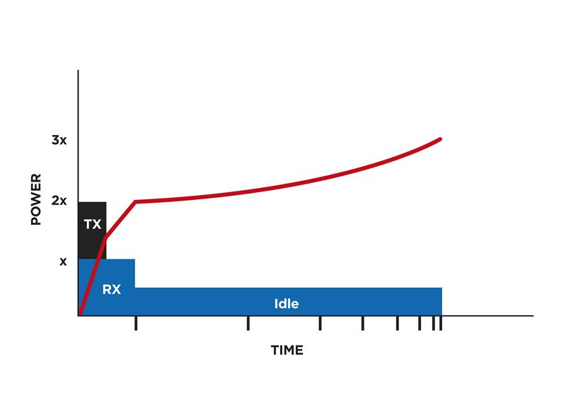
The problem that faces the engineering team trying to optimise the energy consumption of an IIoT sensor node is that many of the design decisions interact with each other. And there are often hidden complexities of designs that lead to energy consumption being much higher than expected. For example, conventional wisdom points to the power consumption of an RF transmitter being a major influence on total energy. But, even though the receiver element may consume far less instantaneous power, system-level decisions that call for the device to listen for intermittent updates from a server can lead to it being left active for long periods of time – tens of seconds per hour versus tens of milliseconds for the transmitter. Because of the long operational life of a typical IoT sensor node, the energy used even when subsystems are sleeping can be responsible for a heavy drain on the battery.
Despite the complex interaction between application design and implementation, there are some high-level choices that are likely to lead toward an optimal solution. One of these is the use of integration. Although it is entirely possible to use 2D-IC and 3D-IC multi chip packaging to assemble a compact IIoT sensor node from off-the-shelf components, integration into a single custom integrated circuit (IC) provides not just significant benefits in terms of cost and size but reductions in power consumption. In order to communicate with off-chip memories and analogue and RF on traditional PCB-based implementations, Input/Output (I/O) drivers with significant current draw are often required. A single system-on-chip (SoC) makes it possible to remove such power-hungry circuits.
The other fundamental consideration for designing energy-efficient IIoT sensor nodes is an understanding of the duty cycle and its impact on lifetime energy consumption. Simply minimising the power consumption of individual elements is not enough to guarantee that a remote or inaccessible sensor can operate on a single battery charge for a decade or more. In such a situation, every microjoule the node requires from its battery is important. But that does not mean the system powered by a typical battery can consume no more than a few microwatts at any point in its life. Such a system would not be able to take measurements and communicate them wirelessly in any practical way.
The use of duty-cycle planning makes it possible for the system to perform tasks that take significant amounts of power for short periods, trading those bursts against savings that can be made while much of the system is quiescent. For example, the RF subsystem of a wireless sensor node need only be powered when it is active. This is likely to be one of the most power-hungry parts of the overall design because of the need to supply enough transmitter power to ensure packets of data can be delivered reliably. However, the power consumed by the transmitter portion of the RF subsystem is relatively easy to control. Once a packet has been delivered the transmitter can be shut down. But there can still be significant power drawn by subsystems such as the RF receiver that continue to remain active once the transmitter has finished sending.
The RF receiver often needs to remain active because of timing uncertainty and this type of uncertainty has a major influence on overall energy consumption. Whereas the transmitter has predictable requirements – it need only be activated when data is ready to send – the receiver needs to be active for much longer. It needs to wait for acknowledgments from nodes to which it is sending data, and also needs to activate periodically to be able to listen for unsolicited messages. As a result, the overall energy consumption of the RF receiver will often exceed that of the transmitter over the lifetime of the sensor, even though its instantaneous power demand is lower. An efficient design will exploit power-saving techniques such as putting much of the circuitry into a low-activity state until an RF signal is detected. Another optimisation is to reduce the amount of time per minute the receiver is active at the cost of the sensor node’s responsiveness to external commands.
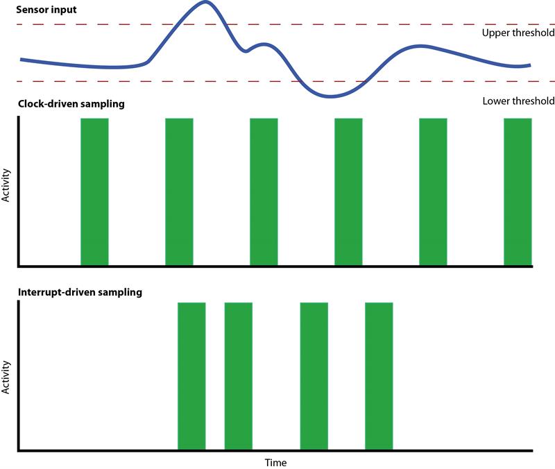
Although they might appear to be essential to all operations, the microprocessor core and its memory subsystem need careful duty-cycle management because they can demand very high levels of power. The problem for many designs is that software running on the processor is often responsible for core tasks such as fetching data from sensors and passing messages to the RF subsystem. This appears to mandate that the processor be fully active whenever sensor inputs need processing.
However, in many cases, the work performed by the software is very simple. It is quickly checking data values to see if they have passed a limit that might signal a problem, or for increased activity that needs closer inspection. Activating the processor to handle all the data is wasteful and can easily be offloaded to custom hardware or a programmable state machine. These circuits consume far less power and can run independently of the processor, so that and the memory array can be powered down.
Current leakage
Even when most of the device is powered down, the power drawn during lengthy periods of sleep can be surprising. Energy lost through current leakage in subsystems that need to remain powered can incur a heavy overhead when analysed over the lifetime of the system because the time the system spends sleeping can be orders of magnitude longer than that during which the system is active. The problem of leakage calls for design techniques that limit leakage in subsystems such as real-time clocks and interrupt controllers to the nanoamp level. It might seem reasonable to disable interrupts for external events and only keep the real-time clock running in some applications. However, in that design the system needs to wake at regular intervals to check inputs that may incur unwanted energy consumption if there is no overall change to record. If the long-term energy usage of an interrupt controller is low enough, keeping that active to respond to events as they happen may make more sense.
When the processor and memory subsystem are powered down, a key decision is how to manage temporary data. One option is to use specialised retention register and memory cells, at the cost of some leakage power. Another is to put important data, such as calibration values, into non-volatile memory (NVM). This allows values to be restored quickly on restart but allows the leakage-prone SRAM arrays and registers to be powered down fully until then. But NVM choices are not always straightforward.
Processes that are optimised for low leakage and that support high-density NVM options may not have the performance required to support efficient RF modules on-chip. The energy needed for I/O drivers that transfer data to an off-chip RF transceiver may outweigh the power savings and security advantages obtained from implementing NVM on-chip. Careful analysis of the application’s requirements will indicate which choice is better for the custom SoC solution.
For the portions of the design that will be active for much of the device’s lifetime, careful attention to detail is required. Seemingly small details such as choosing to multiplex inputs into an analogue-to-digital converter (ADC) will help determine the architecture of choice for those circuits. A sigma-delta ADC may initially appear to offer a good trade-off between accuracy, energy efficiency and silicon area. But it is not suited to multiplexing. Often a successive approximation (SAR) architecture offers superior performance for industrial sensor signals. Advances in SAR design have pushed the energy per bit per conversion down into the range of tens of femtojoules.
Front-end analogue circuits are just as important as the ADC. Amplifiers and buffers that isolate and condition signals before conversion can consume high levels of power and they will be active for long periods of time. Analysis of the specific requirements for bandwidth and accuracy often allow for optimizations that reduce the energy of front-end circuitry and ADCs.
To tie all the subsystems together into a working custom SoC demands the use of power-aware design methodologies to ensure subsystems and circuits are activated properly when required, and can be powered down without disrupting the operation of other parts of the custom IC that need to stay running. Standards such as the Unified Power Format (UPF) have been designed to support such power-aware methodologies, but their application requires experience and attention to detail at different levels of abstraction.
For example, there may be a logical connection between two subsystems that demands they be active at the same time. But physical restrictions may call for them to form part of a larger power island – an area of the mixed-signal ASIC with a common set of power and ground rails – that includes other subsystems that are not required during that time. Design verification needs to ensure that the entire island is powered up correctly. If not, the final SoC will fail. Such physical design considerations may call for changes to the power-control architecture if the consumption of the whole island is higher than the budget allows. It may call for subsystems to be assigned to different power islands, for example.
Verification also needs to pay attention to on-chip noise, which may point to further optimization of the power-island strategy. For example, a low-noise LDO may be used to power sensitive mixed-signal sections that operate autonomously. Once measurements have been taken or RF communications have been completed, a higher-efficiency DC/DC converter may then be reactivated to analyse incoming data and make decisions.
Although the core requirements of energy efficiency in IIoT sensor nodes are readily understood, as can be seen, the implementation choices are complex and often subtle. Many factors affect the optimum solution for a given IIoT sensor node application, although a custom SoC will frequently be the best target in terms of energy and overall cost. Therefore, the ability to call on the expertise of design teams with extensive experience in custom mixed-signal IC implementation is key to success.
Author profiles: Noel O'Riordan is a Senior Staff Design Engineer and Tommy Mullane a Senior Systems Architect, at S3 Semiconductors.


