
Though the space industry has needed to deal with cold electronics for decades, there is a renewed impetus for making electronic circuitry work below the –40°C limit of the traditional extended temperature range that comes from applications much closer to home.
If anything, up to a point, CMOS performs better when cold than when allowed to heat up. The subthreshold swing, which contributes to power dissipation during switching, reduces with temperature. There is less scattering of carriers caused by vibrations in the crystal lattice, which helps improve mobility. And leakage current falls.
Server operators have taken advantage of cooling-derived changes by submerging entire racks in liquid coolant to eke out more gigahertz from high-end processors. However, few have wanted to push CMOS further than the sublimation temperature of dry ice as normal circuit-design techniques begin to break down the closer you head to absolute zero.
Even for deep-space projects, designers have often avoided trying to deal with such extreme operating conditions. They could simply harness the heat that comes from the radioactive sources that are used to generate the electricity for long-lived probes. The Cassini probe sent to explore Saturn’s rings and moons contained almost 150 individual radioisotope heaters, each one about the size of a tube of mints, though significantly heavier.
Where heating is not an option, the amount of electronic circuitry kept in the cold zone is limited. The James Webb Space Telescope that is due to launch in a matter of days, after many delays relies on keeping one part of the probe warm while the other is kept at 30K, in order to capture faint infrared light from the edge of the observable universe. Teledyne developed an ASIC called Sidecar to digitise the weak signals picked up on the cold side and transfer them to a signal-processing system operating at higher temperatures.
Cryogenic electronics
Much of the past focus on cryogenic electronics has been on circuit designs that practically demand such low temperatures. The Josephson effect uses quantum tunnelling through the thin barrier between two parallel superconducting plates. This tunnelling can be so efficient that up to a given level current will flow freely with no voltage drop.
Force current through the circuit containing the junction that surpasses a critical level and the device oscillates at high frequency. This difference in states provides a way to make the junction work as a switch.
Because of their innately high switching speed, Josephson junctions were once considered as potentially useful devices for supercomputers. But the cost of cryogenic cooling needed to maintain the superconducting state far outweighed the speed and energy benefits of using them. As a consequence, the junctions have been largely confined to niche applications, often based on the superconducting quantum interference device (SQUID), which has found applications in biological and medical instruments as well as radio astronomy because it can detect tiny magnetic field fluctuations.
 Above: A graph from the International Roadmap for Devices and Semiconductors shows the widening density gap between superconductor logic and CMOS
A couple of decades later, interest in superconducting electronics has returned and with the promise of a lot more money. Quantum computers, for the most part, rely on temperatures close to that of liquid helium to maintain the entanglement between quantum bits (qubits) for as long as possible. According to the International Roadmap for Devices and Semiconductors (IRDS), the integrated circuit with the largest number of Josephson junctions on-chip, at just over 1 million, is D-Wave’s Pegasus P16, a computer that performs quantum annealing. This is a type of computer that relies on quantum tunnelling between storage elements to perform optimisations and represents an alternative to the full “quantum supremacy” machines that remain the focus of most researchers into quantum computing.
Today, the experimental machines pushing towards quantum supremacy manage a handful of supercooled qubits able to work on comparatively simple problems. Rather than use supercooled electronics to control them, most designs in use today run long, heavy shielded cables from the cryostat to CMOS ASICs and FPGAs placed some distance away. This not only lets the chips function at normal temperatures it also stops them heating the qubit elements.
As the number of qubits grows, remote-control electronics become far less feasible and R&D teams are now looking to integrate either superconducting controllers into the cryostat or use CMOS able to work at temperatures measured in millikelvin. The big advantage of superconducting circuitry is that it works today. Unfortunately, it is far from area efficient, largely because the devices rely on magnetic components such as inductors and transformers rather than the capacitive elements that make up CMOS circuitry.
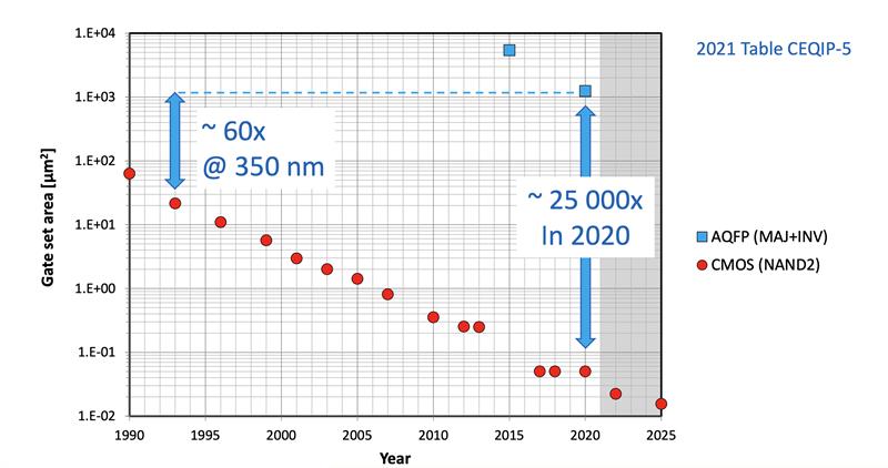
Back in the 1990s, gates constructed from common superconducting logic families consumed 60 times more area than CMOS gates able to perform the same function. Thirty years on, the differential is more than 10,000 times.
One direction that researchers are working on in flux-quantum logic families is to find ways to make them smaller. This may come through an application of the same types of system-technology code sign techniques that have helped bring CMOS dimensions down in the face of a slowdown in conventional Moore’s Law scaling.
Such changes may help remove many of the transformers that sit between individual junctions. Materials changes may help.
Metal of choice
Today’s superconducting metal of choice is niobium. Unfortunately, it suffers from problems caused by very large crystal grains that restrict how small functional elements can be. It also means chips need to be manufactured using lower temperatures than those used to make CMOS transistors, which makes integration hard to achieve.
Though heat transmission from the innate resistivity of CMOS devices may prove to be a problem when trying to design cryogenic systems with high qubit densities, the silicon technology has the distinct advantage of being far more compact even using comparatively mature processes such as 28nm and a far more familiar approach to circuit design. Being a two-terminal device rather than three, the Josephson junctions needs radically different approaches to logic design. On top of this, the need to take inductance into account throughout the circuit is not something handled by conventional EDA tools and greatly complicates the design.
R&D teams today see the biggest obstacle to CMOS in the millikelvin range not so much in manufacturing but in design. The temperature range is way below what conventional simulation tools handle though this has opened the door to start-ups such as UK consortium member SemiWise, founded by Glasgow University professor Asen Asenov. Whereas Asenov’s previous start-up, sold to Synopsys in 2016, focused on the variability issues of nanometre-scale transistors, SemiWise is focused on ultralow-energy and low-temperature devices.
Though many properties improve, the behaviour is different to demand changes in circuit architecture and as the temperature approaches absolute zero, the chances of carriers simply freezing out of the conduction bands increases, resulting in a reduction of current by more than an order of magnitude once a saturated device is supercooled. Though sub-100nm devices can work with comparatively lower voltage as freeze-out approaches, they are affected by variability issues exacerbated by dopant ions freezing out. Similarly, charge traps at the interfaces between the gate and the channel regions play stronger roles in determining how the transistor behaves. However, modelling work combined with test-chip production so far indicates that these effects are predictable.
Another stumbling block might be reliability.
Damage from hot carriers looks as though it will be the dominant failure mode at such low temperatures, particularly for the short gate lengths of sub-100nm processes though some simulations have found that working with longer gates for circuits that are likely to be more affected by the problem could help extend practical lifetime. More modelling work will help. In the case of the UK project, this will go into memory and other IP to support two proposals for quantum computers as the concept inches closer to commercial deployment.


