
One of the main challenges associated with making an ALS for the evolving wearables market, however, is that the ALS device must have an extremely thin form factor as it is usually mounted directly onto the actual flex PCB of the touch panel display. Additionally, the sensor’s accuracy and sensitivity should also be robust enough to allow for mounting behind inked glass.
Light sensor technology has been around since the 1950s, and has evolved from the inception of simple photodiodes and phototransistors to intelligent opto-sensing solutions, which offer a much higher level of integration, lower operating power and inclusion of noise immune digital bus interfaces. These modern day ambient light sensor solutions incorporate photodiodes, analogue-to-digital converters (ADC), control logic for interrupt persistency and thresholds events, and a fast-mode I2C digital interface. The digital interface and interrupt capability makes it well suited for use in microcontroller and processor based applications such as wearables and smartwatches.
As shown in Figure 1, ALS sensors are connected through a digital I2C interface to an applications processor in the smartwatch block-diagram.
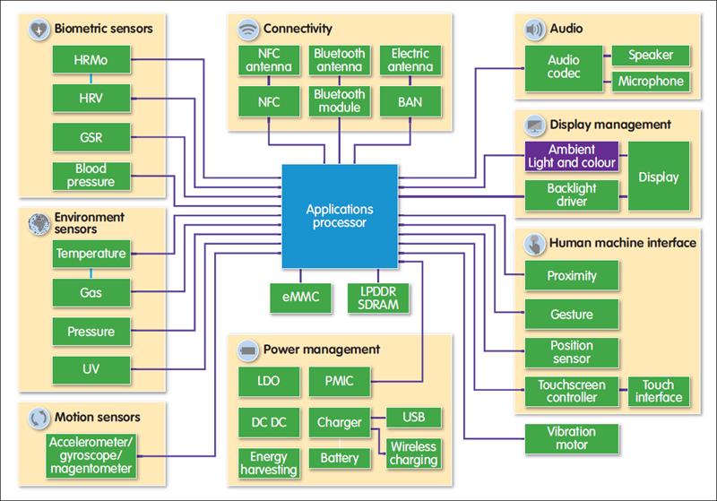
Figure 1: Smartwatch block diagram
Photopic and silicon response
As with most consumer electronic devices, including wearable products, cost-effectiveness is a key factor. Therefore, a light sensor made with a CMOS photodiode offers the effective solution. However, the spectral responsivity of CMOS silicon is between 300nm and 1100nm, and peaks at around 700nm in the Infrared (IR) region. As shown in Figure 2, the human eye responds to light in the 390-750 nm wavelength range.
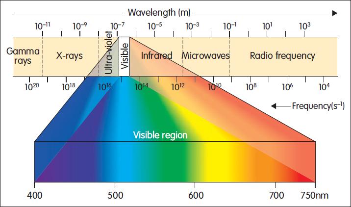
Figure 2: Visible Light Spectrum
As seen in Figure 3, the visible region that the human eye responds to light encompasses a small portion of the region of the photodiodes response.
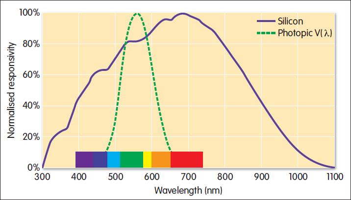
Figure 3: Silicon responsiveness and the photopic response
The challenge of making a robust ALS is getting it to see the same 390-750nm wavelengths that the human eye sees without responding to wavelengths in the 300-390nm Ultra-Violet and 750-1100nm IR wavelengths.
The TSL2584TSV light-to-digital sensor from ams, views ambient light just like the human eye sees light.It uses a very-sensitive Analogue Front-End (AFE) with a patented dual-diode architecture to transform light intensity into a digital count value.A broadband photodiode responsive to visible and infrared is used in conjunction with an infrared-only responsive photodiode and the two photodiode channel responses are mathematically subtracted via a lux equation on a micro-controller through the digital I²C interface. Ambient light level illuminance in lux is derived using an empirical formula to approximate the human eye response.
In Figure 4 below, the TSL2584TSV is shown:
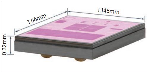
Figure 4: TSL2584TSV photos
To optimise this ALS solution, the TSL2584TSV includes an on-chip photopic infrared-blocking interference filter that rejects un-wanted UV and IR producing a near-photopic response.This produces a highly accurate lux measurement irrespective of glass transmissivity, even when mounted behind very dark opaque glass. Through advanced filter deposition technology ams produces a more accurate and repeatable photopic filter than other filters offered in the market.This photopic filter virtually has no temperature or humidity variation and is deposited directly onto the silicon.The TSL2584TSV spectral responsivity is illustrated below:
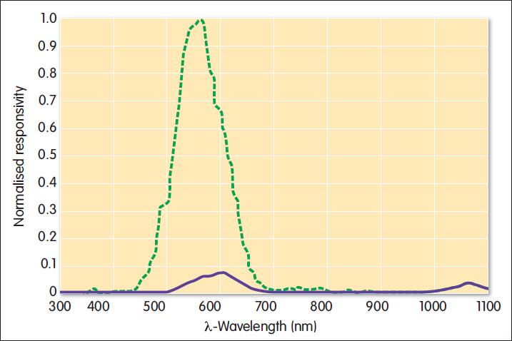
Figure 5: TSL2584TSV Spectral response
TSV technology
With the advantage of having in-house wafer fabrication expertise, through-silicon via (TSV) packaging technology has been adopted by ams for advanced light sensor technology. TSV technology eliminates the use of wire bonds and provides a direct connection from the device I/Os to a solder ball as shown in Figure 6 below.
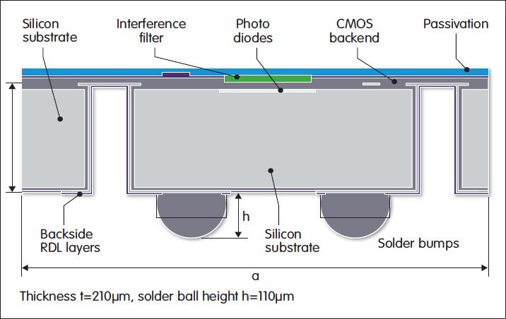
Figure 6: Through-Silicon Via packaging technology
The small package size of the TSV package technology, addresses the small form factor size requirement in wearable products. The TSV package technology which has been developed and qualified by ams enables the design and production of radically improved IC packages that are smaller and offer better device performance.
As seen in Figure 4, the TSL2584TSV ALS has a very small package size of 1.145 x 1.66mm with a height of 0.32mm which is approximately half the size of competing devices and makes it the world’s smallest ALS.
The TSV technology uses an etched via through the TSL2584 silicon wafer. Tungsten is deposited into these etched cavities, a Backside Re-Distribution Layer (BRDL) is deposited from the via to the planned solder ball location, then SAC305 (Sn96.5Ag3.0Cu0.5 alloy composition) or similar Pb-free solder balls are affixed which results in an overall package height of 0.32 mm.
Removing the wirebonds and routing the signal directly down through a via channel constructed during the silicon manufacturing process results in an overall package height reduction, as seen in Figure 7. In addition, without a bond wire connecting the IC to the package, interconnect inductance is minimised.
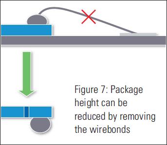
Figure 7: Reducing package height by removing the wirebonds
Another key feature of this TSV package is that it is offered in a glassless package, which helps to further reduce the overall z-height compared to chip-scale packages. Since there is no actual glass material included in the TSV package, not only is the z-height reduced but this type of glassless package is ideally suited for use in a different product to enable UV detection when paired with UV pass filters.
Device reliability performance is also significantly improved with the TSV package because it minimises the corrosion effects due to humidity exposure and enhances temperature-cycling performance. The TSV package has interconnects internal to the package, unlike some chip-scale packages that require metal edge connections, thus improving reliability of the TSL2584TSV to a Moisture Sensitivity Level-1 standard rating making it suitable for higher moisture environments.
The photopic interference filters deposited on the TSL2584TSV are quite dense, are extremely durable and have highly scratch resistance characteristics, similar to the glass used in chip-scale and MEMS packaging. The spectral response of the photopic filter has no degradation or spectral shifting after Highly Accelerated Stress Testing because its filter characteristics are not sensitive to Temperature and Humidity variations.
Future outlook
The wearables market is in its embryonic market state with just 24million smartwatches and fitness band shipments in 2014. In a recent report from BI Intelligence, this market is projected to grow at as much as 35% CAGR to 135million units by 2018.
As the wearables market continues to evolve, offering reduced size, accurate, and high sensitivity ALS solutions such as the TSL2584TSV enables designers of wearable devices such as smart watches and fitness bands, to easily integrate ambient light sensors into the thinnest backlight displays. Improved accuracy and sensitivity performance allows for mounting behind inked glass while automatically controlling the backlight intensity and ensuring the best user experience. The ultra-small size of the TSL2584TSV provides developers with increased design flexibility as its footprint is less than 2mm2 and has a height of only 0.32mm and overall a robust and effective solution.
Author details:
Dave Moon is Senior Product Marketing Manager (US), ams AG


