
Modulation is a process by which characteristics of a high-frequency carrier signal are altered to convey information contained in a lower-frequency– or baseband – signal. Modulation is based on the fact that by “mixing” or “beating” together two signals at different frequencies, two products are obtained – one waveform at the sum and a second at the difference of the two frequencies.
An example of modulation is shown in Figures 1 and 2, which illustrate amplitude modulation, (AM) in the time and frequency domains. The information – or baseband – signal is mixed with the high frequency carrier (RF) signal before transmission, resulting in the amplitude of the carrier frequency varying according to the baseband signal.
In the frequency domain the result is a double-sideband signal, centred on the carrier frequency, with twice the bandwidth of the original signal. By careful choice of the carrier frequency, the modulated signal is shifted to the required point in the frequency spectrum – usually allocated by the relevant regulator, e.g. for radio stations, etc. The other two main types of modulation are frequency modulation (FM) and phase modulation (PM). Several other methods exist which are based on combinations of these basic types.
The main function of a radio receiver is to capture the transmitted RF signal and recreate the original baseband signal – a function known as demodulation, effectively the reverse of modulation, where the baseband signal is recovered from the carrier signal. AM demodulation is usually carried out using either rectification or filtering techniques whereas, in modern radios phase-locked loops, (PLL) are used to demodulate FM signals.Modulation enables the more effective use of spectrum by ensuring transmission within the allocated frequency band, and more efficient transmission as radio signals propagate more effectively at higher frequencies.
Classic radio receiver design has been based around the superheterodyne approach where the RF carrier is down-converted to one or more intermediate frequency (IF) stages before being demodulated – as shown in Figure 3.
There are several advantages to using this approach:
• By tuning the local oscillator (LO) according to the received RF signal, (ganged tuning), common IF frequencies can be achieved, which simplifies subsequent processing.
• Filter bandwidths increase with frequency, consequently, it’s harder to eliminate unwanted signals at RF frequencies than at IF levels.
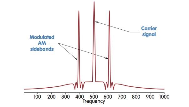
Figure 2: Frequency domain of an AM signal |
Classic AM and FM techniques have been unable to meet the growing demands for high-volume traffic as modern communications systems demand more information capacity, higher signal quality, greater security and digital data compatibility. Recent technological advances have been instrumental in addressing these challenges.
I/Q modulation is one of a number of new modulation methods, when combined with other digital techniques, that enables more efficient use of spectrum and handling of digital data as well as voice.
I/Q modulation uses two carrier signals; the in-phase (I) and quadrature (Q) waveforms, with the Q waveform being generated by shifting the I waveform by 90 degrees.
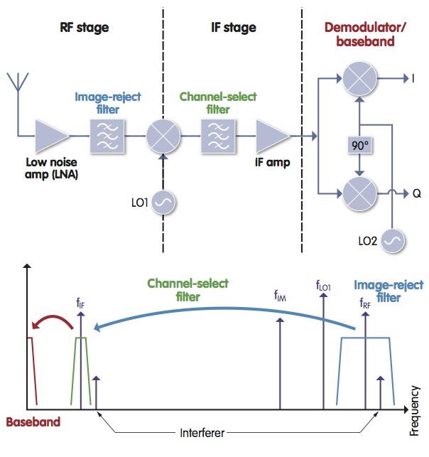
Figure 3: Superheterodyne receiver |
Each waveform can be modulated separately enabling the creation of a variety of different modulations.
Direct Conversion (DC) receivers have emerged to meet the growing demand for smaller radios that offer lower power consumption, for applications such as mobile telephony and IoT applications.
DC, which also employs I/Q modulation, involves down-converting the RF signal directly to baseband in a single stage by matching the LO frequency to the RF carrier frequency. This technique removes the need for the bandpass filters required in superheterodyne receivers, resulting in a more compact receiver.
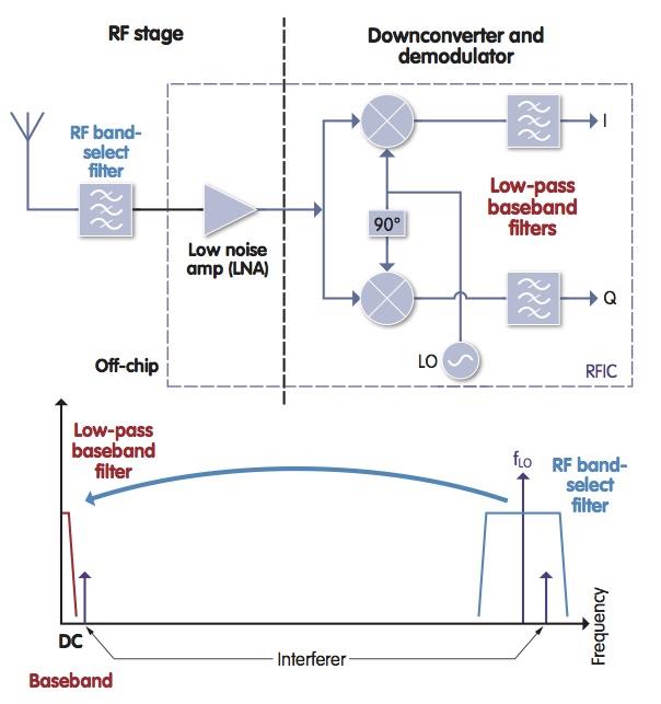
Figure 4: Direct conversion receiver |
Although the origins of DC can be traced back to 1924, it’s only over the last 20 years or so that market forces, combined with the development of semiconductor process technologies, have enabled this technology to gradually supplant superheterodyne designs.
Figure 4 shows the basic structure of the DC receiver.
A single local oscillator is used to shift the incoming RF signal down to baseband. Baseband contains two paths, I-path and Q-path, corresponding to in-phase and quadrature paths. Each path is then digitised separately.
The two variants of DC are near-zero IF – where the LO frequency is slightly different from the carrier – and low IF, where the difference is a little greater, but not as great as that used in a superheterodyne receiver.
The Challenge
Although the DC receiver has benefits over the superheterodyne receiver in terms of bandwidth and compactness, implementation of this technology does face a number of challenges:
• I/Q imbalances: Can occur due to slight mismatches in sections of the receiver chain when dealing with the I and Q signal paths. These mismatches can occur if there is any variance in the 90 degree delay between I and Q signals and can also arise from any slight mismatch in overall gain for each of the signal paths. These imbalances need to be corrected over both frequency and temperature.
• Non-linearities: Higher (2nd and 3rd) order intermodulation products, derived from strong out-of-band interference or blocking signals can produce harmonics and intermodulation terms, which will then appear in the baseband. In DC, second-order non-linearity of the mixer is critical, as it produces baseband signals that appear as interfering signals in the down-converted desired signal. This can be alleviated by extremely well-balanced circuit design.
• DC offset: A strong, nearby signal, including the receiver’s own LO, can mix with itself down to zero-IF (this is known as “self-mixing”) and generate a DC level appearing as interference at the centre of the desired band. As well as interfering with low frequency components in the desired baseband signal, DC offset changes the average voltage of the signal waveform, as shown in Figure 5, leading to issues with the dynamic range of the ADC convertors.
Figure 5: Waveform with DC Offset |
The Solution
DC receiver architecture has become an attractive solution for meeting the demands of the commercial market for low-cost, low-power, wide bandwidth, and highly integrated RF circuitry.
CML’s CMX994/A/E family of DC receivers are designed to provide exceptional interference immunity, in terms of second order intermodulation and blocking, suitable for professional radio designs, whilst also offering low power modes. DC offsets are handled in several ways; the receivers are specified with a typical mixer IIP2 performance of +79dB, which attenuates any second order mixer intermodulation products appearing at 0Hz (DC). A commonly used DC offset correction method in DC receivers is to apply small correction voltages at the mixer outputs, before the baseband signals are amplified. The CMX994 devices enable this using an on chip register – the Rx Offset register – which can be accessed by the microprocessor or DSP that processes the I/Q signals from the CMX994. Access to the register is via the device’s C-BUS interface and the value of offset applied is controlled by the 8-bits in this register.
The offsets applied to I and Q signals are independent, with bits 0 -3 controlling the offset applied to the I Channel and bits 4 – 7 controlling the Q channel. Since the level of DC offsets can vary with frequency and gain, a number of measurements should be taken, ideally without a signal being present, whilst setting up the system. The signal processing algorithm can then be set up accordingly in order to apply the correct offset voltages during operation.
DC conversion presents a solution for high performance, low power and low cost radio receivers with fewer filters and a lower bill of materials than the traditional superheterodyne design. This enables a high level of silicon integration, while recent advances in technology have enabled designers to overcome many of the challenges inherent to DC conversion.
Author details: Nigel Wilson is CTO at CML Microcircuits |


