
Modern FPGA devices feature integrated microprocessor cores, digital signal processing (DSP) units, memory blocks and other specialised intellectual properties (IPs) and these advanced devices allow for the implementation of large, high-performance system-on-chip (SoC) designs with integrated safety mechanisms, making a strong case for adoption in additional safety-critical applications traditionally dominated by application-specific integrated circuits (ASICs).
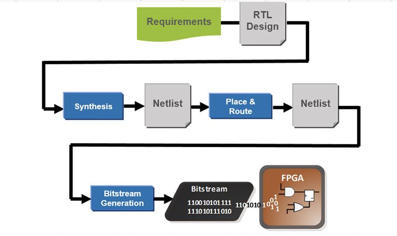
From a high-level perspective, the FPGA and ASIC development flows are similar. Register-transfer level (RTL) coding and integration of third-party intellectual properties (IPs) are crucial steps in the front-end part of the flow. Extensive functional verification of the RTL design model reduces the risk of mismatches between requirements and RTL behaviour. At this stage, specification, coding, and module integration mistakes are the main source of systematic faults that, if undetected, could lead to dangerous failures of the FPGA device in the field.
The RTL model then goes through several implementation steps (see below). Synthesis and place-and-route tools map the design onto the target FPGA device. The bitstream generation step produces the file used to program the FPGA. Functional verification of implementation steps reduces the risk of mismatches between the derived netlists and the RTL design model. This is crucial to close the loop and ensure that the functionality implemented in the FPGA device matches the hardware requirements.
 Above: The FPGA development flow
Functional bugs can be introduced during implementation steps, either because of RTL issues that cannot be detected during synthesis, or because of malfunctions in implementation tools, particularly synthesis and place-and-route, corrupting the original RTL functionality. While engineers may expect that implementation tools have been extensively tested prior to release, each design and coding style are unique and may trigger unknown corner cases.
Regardless of the implementation tool used, there are coding issues that may go undetected during RTL verification and creep into the synthesis
netlist. In some corner case scenarios, RTL simulation behaviour may not match the behaviour of the corresponding netlist in the presence of unknown, or X, values. Consequently, while the synthesis tool operates correctly, its generated netlist may still not match the intended RTL behaviour.
Requirement-based testing does not explicitly target these type of corner cases, which can therefore be missed. RTL linting tools may warn about these scenarios. However, they provide neither a definite answer nor a simulation trace that shows how the bad scenarios may occur.
Desired functionality
FPGA implementation tools must fit the desired functionality into a prefabricated structure while meeting performance and power consumption goals. Implementation tools perform significant changes to the original logic structure of the design to improve device utilization and overall quality of results (QoR). Advanced optimisations pose a higher risk of corrupting the RTL functionality.
Certain FPGA synthesis tools support the automatic insertion of hardware safety mechanisms. Safety mechanisms shall not change the design functionality when no fault is present. In the event of a random hardware fault occurring during field operation, they need to raise an alarm and potentially correct the effects of the fault on the fly.
Synthesis tools may transform the encoding of finite state machines (FSMs), for example to include Hamming-based error detection and correction. Triple modular redundancy (TMR) is another type of safety mechanism where a critical logic function is triplicated and voting logic added to determine which of the three outputs should be considered as correct. Logic duplication and inference of memories with error correcting codes (ECC) may also be supported. Users certainly benefit significantly from these design enhancements that can be performed automatically by the synthesis tool. However, the inserted logic could contain bugs and must be rigorously verified.
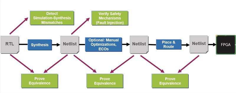
An effective verification flow must detect bugs as soon as possible once they are introduced. Detecting an RTL issue or synthesis bug during lab testing or Gate Level Simulation (GLS) of the place-and-route netlist is inefficient. Moreover, the effect of bugs introduced by implementation tools is unpredictable. Simulation tests are not intended to verify the correctness of the implementation tools, and even running all available tests at gate-level only provides limited confidence. This approach is indeed far from exhaustive. Finally, debugging GLS and lab test failures is hard and time consuming.
Formal methods are widely recognised as a powerful and exhaustive verification technology. Formal design inspection and exploration is valued for detecting both basic and corner-case RTL issues early and without the need for a simulation testbench.
Automated, formal inspection of RTL code detects issues before synthesis starts. Unlike linting, formal tools provide a definite answer on whether an array may be indexed out of bounds. In this case, the tool provides an easy-to-debug simulation-like trace, or counterexample, that demonstrates how the design misbehaves.
EC tools
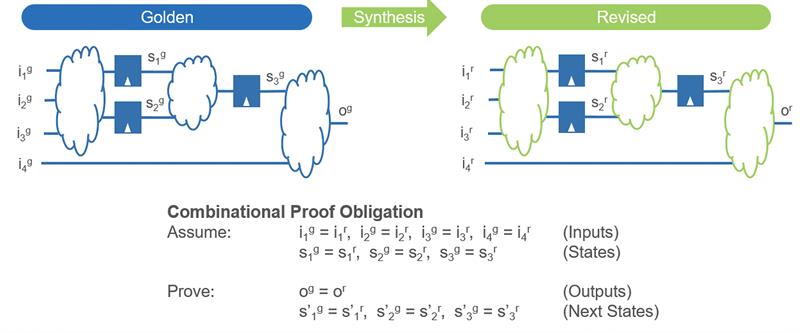
Formal EC tools can mathematically prove (or disprove) that two designs are functionally equivalent. This is the most rigorous way to ensure that synthesis and other implementation steps have not introduced bugs. The input design to the implementation tool is typically named golden design. The generated netlist is named revised design.
Combinational EC largely relies on one-to-one mapping of states between golden (e.g., the RTL) and revised (e.g., post-synthesis netlist) designs. Through state mapping, the complex problem of proving that two large designs are functionally equivalent can be split into a multitude of much simpler problems: comparing the functionality of two combinational logic cones.
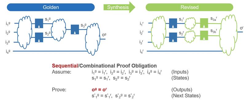
 The design transformations performed by FPGA implementation tools significantly break one-to-one state mapping. Formal sequential EC algorithms can prove equivalence of sequential logic cones, thus not requiring state mapping. However, while these algorithms have improved dramatically in recent years, they do not scale. Partial state mapping is necessary to leverage combinational EC wherever possible and apply sequential algorithms only on limited design portions. In this context, identifying corresponding states is a crucial, challenging task. Manual mapping is tedious and time-consuming. Mistakes waste engineering resources.
 Above: These figures show proof obligation in sequential and obligational equivalence checking
Formal verification signoff enables engineers to use advanced FPGA optimisations and the latest synthesis technology with confidence. Formal RTL design inspection is more powerful than linting and finds issues early, prior to synthesis. Formal EC proves that the golden design functionality is not corrupted by the implementation step. Finally, formal fault injection and verification supported by specialised safety tools, can automate the verification of safety mechanisms in the scenarios when faults occur. With this flow, weeks of GLS and lab testing can be replaced with hours of formal tool runtime.
FPGAs have long been the hardware platform of choice in many low-volume safety-critical applications. Nowadays, these devices can implement complex functions while fulfilling tough performance and power goals, competing with ASICs also on high-volume safety-critical applications, including automotive.
The availability of advanced EDA tools and methodology is crucial to support this trend. ASIC development has used formal EC for nearly 20 years. Automated formal checks prior to synthesis are also widely adopted by ASIC teams. The same technology is now available in FPGA development, enabling a robust, efficient implementation process. OneSpin’s formal signoff flow of FPGA implementation has been designed to be orders of magnitude more rigorous and efficient than GLS and lab tests. The technology is mature and proven on hundreds of industrial designs for communications, NPPs, and other safety-critical applications.
Author details: Rob van Blommestein, Vice President of Marketing, OneSpin Solutons


