
Replacing mechanical pumps with electric motors delivers direct benefits – they can be turned off when not needed, deliver energy savings and improved engine performance. Cold engines that aren’t cooled as soon as the engine starts will reach their optimum operating temperature sooner, burning fuel more cleanly. Speed dependent features, such as power steering are also easier to implement and are more reliably controlled electronically.
Electric motors have had an impact on vehicle design. Engine control units (ECUs) have become more complex and, while BLDCs have well documented advantages over their brushed based cousins, there are ‘hidden costs’, such as the more complex control electronics needed to drive them.
Despite this, migration to BLDCs in the automotive industry is accelerating.
As a result, BLDC drive and control design is coming under closer scrutiny. While the basic methodology can be grasped, the finer details demand greater care. Add to this the concept of sensorless control, the particular demands of the automotive industry and component selection, it becomes clear that, from a design standpoint, the move to BLDC motors presents specific challenges.
Smoothing transition
MCUs have helped bring BLDCs to the fore, thanks to the ability to integrate the algorithms needed to control a BLDC motor with the peripherals needed to drive it.
Typically, an MCU drives power MOSFETs directly or through gate drivers, arranged in a topology that allows excitation of the three coils used in three phase BLDC motors.
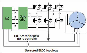
BLDCs don’t use brushes to complete the circuit within the motor. Instead, force is induced by employing position detecting algorithms and/or Hall-Effect sensors to energise the coils in the right order. As there is no physical electrical connection to rotating parts, electrical arcing is eliminated, as it the limitation to the amount of torque that can be generated. With a BLDC motor, torque is limited largely by the MOSFETs used to direct the current. These features make BLDC motors more appealing where high torque, high rotational speed and greater control over both is desired.
It is also clear that correct selection of the MOSFETs is paramount, particularly in relation to reliability, efficiency and design.
Directing current
Control circuits for three phase BLDC motors – which feature three coils – use three half bridges, where the MOSFETs are employed to direct current through the appropriate coils based on the motor’s rotational position and required direction. The MOSFETs are typically driven by a PWM signal, which switches the transistor(s) off and on at the correct times to induce rotation.
A full bridge driving a single phase is shown in Figure 2. In this topology, MOSFETs are connected such that a path is created between the power rails through two MOSFETs and the coil. The way in which the MOSFETs need to be connected means that, during transitions, a short circuit can exist between the power rails without passing through a coil. Clearly, if this were to exist for any significant period of time, the MOSFETs could suffer catastrophic damage. For this reason, a small time period – ‘dead time’ – is implemented between turn off and turn. During this dead time, the body diodes of the MOSFETs will conduct. Stages 2 and 4 in Figure 2 show the dead time intervals in the commutation sequence. Minimising dead time is the overriding objective of the control algorithms and that will be determined by the switching parameters of the MOSFETs used.
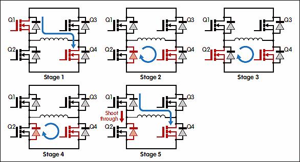
As a result of accommodating a safe dead time, another phenomenon –reverse recovery current – is seen in the MOSFETs’ body diode. This residual current flows through the body diode during dead time and throughout the MOSFETs’ switch-on/off periods. The body diodes will continue to conduct, even when reverse biased during the commutation sequence due to stored charge. For a short time, this creates a momentary shoot through, which also introduces switching losses and EMI, and lower overall efficiency (see stages 4 and 5 in fig 2).
The body diode effect influences maximum operating frequency and, when combined with the circuit’s parasitics, introduces further losses and in some case voltage transients. Choosing a MOSFET with a fast recovery parallel diode can help optimise the design, as does using an MCU and algorithm that can minimise dead time.
The path of lowest resistance
MOSFET on-resistance (RDS(ON)) is used to steer the current through a motor’s coils and can introduce significant losses; something designers strive to minimise. N-Channel MOSFETs are normally selected since typically they exhibit half the RDS(ON) of P-Channel devices of the same die size. However, RDS(ON) is dynamic; it changes during operation a result of the voltage across its gate and source terminals, the current flowing through its channel and, perhaps most significantly, the temperature of the device itself.
To achieve low RDS(ON), a large active area N-Channel MOSFET is required, but the larger the device the higher the gate charge exhibited. This makes the transistors slower to switch on, thereby limiting their operating frequency. One method employed is to lower RDS(ON) is to increase the trench density of the device. But while this does lower the on-resistance, it also increases the Zero Temperature Coefficient (ZTC) point of the device.
This is important because a MOSFET should operate with a gate voltage above the ZTC point. This point will be documented in the data sheet, with a transfer curve of drain current (ID) against gate-source voltage (VGS). The curve shows two regions of operation; a positive temperature coefficient region and a negative temperature coefficient region for the gate voltage. Operating with gate voltages below the ZTC point can introduce the possibility of a temperature-related failure.
By understanding and designing for this parameter, the MCU generating the PWM switching waveforms can be configured to deliver the optimal gate drive voltage.
The rise of BLDCs has been enabled by modern microelectronics and advances in power MOSFET design but it is arguably the MOSFETs that now differentiate an adequate design from an excellent one. MOSFET selection must be made with an appreciation of design parameters under application conditions.
The unique operational environment of the automotive sector imposes significant demands on performance and meeting these while still delivering energy savings will require careful component selection.
Author profile:
Siva Uppuluri is an applications engineer with Diodes.


