
Kahng’s precise structure would never go into production, but his floating-gate idea would resurface as the key element in EEPROMs. Instead, the foundation for modern charge-based non-volatile memories followed work by Eli Harari who, while at Hughes Microelectronics, filed his patent for the first practical floating-gate EEPROM in February 1977. It provided a more convenient but expensive, alternative to the EPROM developed by Intel, but wound up being relegated to being an EPROM companion for configuration data.
Two decades later, Toshiba started a revolution that reinvigorated the EEPROM and which is now eating into the magnetic disk drive market. At the International Electron Devices Meeting in December 1987, Fujio Masuoka and colleagues unveiled a type of EEPROM that could be made more cheaply. The NAND flash would prove to be cheaper than the NOR flash devices that Masuoka had already developed and which would arrive on the market in 1988.
NAND flash packed multiple bits into strings that follow the bitline of the memory array. This reduces the amount of metal interconnect used to wire up the memory transistors, more than halving the area of the unit cell compared to NOR flash. This comes at the cost of slower and more difficult access to individual bits. But the lower cost and similarity to the serial streaming of a magnetic disk drive means that, 20 years later, flash has challenged the magnetic disk drive’s dominance. That in turn continues to drive the need to increase capacity.
But flash is a storage technology that relies on the measurement of charge to function and, by 2007, seemed to be heading into the Moore’s Law wall well before other IC technologies.
Although lithography technologies, assisted by immersion and double-patterning extensions, could define the onchip features readily, the memory’s own mechanism conspires against it at ultrahigh densities in two ways. One is interference between adjacent cells as the data values inside each cells are rewritten. The other is simply the amount of charge that a scaled-down gate can hold. At less than 30nm – even with high-k dielectrics – the amount of charge drops dramatically because the tunnel oxides that hold the electrons need to be extremely thin. Variability in threshold voltage compounds the problems.
As the 32nm generation was heading towards manufacture, Toshiba said, in June 2007, it had found another path to push production costs down and avoid the 2D-scaling problems. The idea of moving into the third dimension is one which the rest of the IC industry may follow. However, the regular array of a memory coupled with the string-centric nature of the NAND architecture makes it a natural fit for 3D structures.
Early work on 3D NAND followed the same path as that being pursued for stacked logic and non-flash memories, such as magnetic and phase-change RAMs. These build layers of memory elements one at a time. The downside of such an approach is that the wafer stays in the fab longer, with many more processing steps – all of which add significantly to cost and yield loss. Another problem is that simply adding layers to the planar architecture would tend to increase the number of driver transistors needed to implement control gates – they would need to be replicated on each layer.
Toshiba’s approach had cost as its primary motivation – tagging it ‘bit cost scalable’ (BiCS) – and took the novel approach of rotating the string so that it extended vertically from a select gate on the base layer of the wafer. In principle, the approach promised an instant 16-fold increase in bit density in one step.
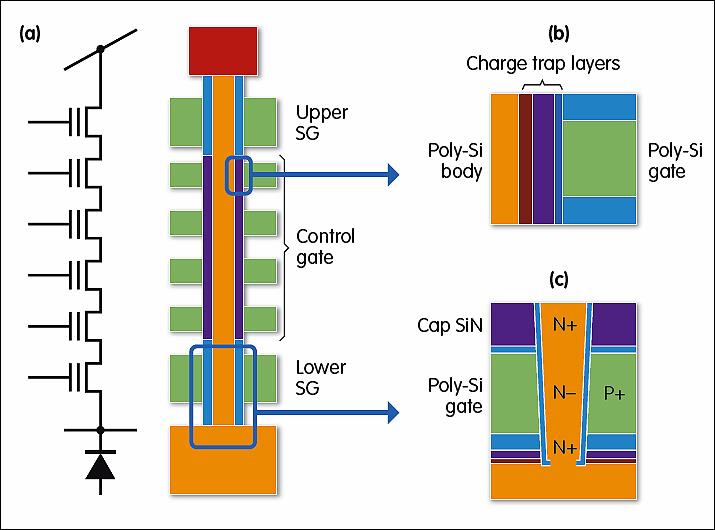
The beauty of BiCS is that it deposits complete sheets of polysilicon on top of the wafer that end up being used as wordlines to address individual cells. In between each polysilicon layer is an insulator, such as silicon dioxide.
Once the sandwich has been formed, using processes that are relatively cheap and easy to control in a modern fab, the next step is to punch an array of holes down to the layer of control gates. This takes advantage of another cheap and surprisingly delicate and controllable process technology – dry etching. Today’s fab equipment can form holes with an aspect ratio of 60:1 or more and the walls of each hole will be almost vertical. That hole is filled with materials that form not just the bitline, but also nitride and oxide regions that allow charge to be trapped and stored.
In the original BiCS architecture – and in subsequent devices made by Spansion and Samsung – there is no floating gate. Instead, the arrangement of nitride and polysilicon at each layer forms a charge trap region that is joined physical to its neighbours but which, in an ideal device, does not allow the charge to leak from one region to another. But depositing material in layers evenly inside the deep, narrow holes is not easy. And it puts a limit on how small the holes can be.
In 2009, Samsung came up with an approach that switched out polysilicon for a silicon nitride that would then be sacrificed in a process similar to the replacement-gate technique used by Intel on its high-k metal gate transistors. As a result, Samsung’s approach gets tagged ‘gate last’ in contrast to BiCS-like ‘gate first’ processes. In principle, the gate-last approach makes it easier to pack strings side by side, but it has taken novel process engineering to make it work. Because the gate is constructed around the etched-and-filled column, that column only needs to contain conductive polysilicon. The hole can be much slimmer than the one of a gate-first process.
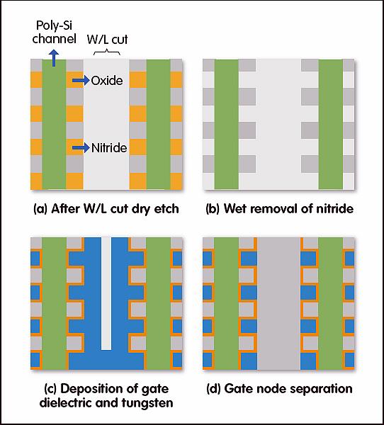
Figure 2: Concept of the gate replacement process flow
For most of the past decade, 3D flash looked to be more of an ambition than commercial reality. But the pace of commercialisation accelerated towards the end of 2015 with Samsung’s decision to use 3D flash for server-class solid-state drives based on a 48 layer structure that stacks several strings on top of each other. Micron quickly followed and, according to analyst DRAMeXchange, both companies now ship more bits in 3D structures than traditional planar designs.
Working with Western Digital, Toshiba started production in late February 2017 of a 64-layer 3D flash that stores 3bit per cell, increase capacity per chip to 512Gbit. For the second half of 2017, SK Hynix is moving to a 72-layer design, having introduced 36- and 48-layer products relatively recently. By the third quarter, DRAMeXchange expects 3D flash to account for more than half of flash bits shipped. With capacity for 2D device now being squeezed as manufacturers switch production, it seems that for flash in 2017 the only way is up.


