
A recently launched project by scientists from the university of Freiburg, the Sustainability Center Freiburg and the Fraunhofer-Gesellschaft is now looking into novel semiconductor material scandium aluminum nitride (ScAlN).
ScAlN is a piezoelectric semiconductor material with a high dielectric strength which is largely unexplored worldwide with regard of its usability in microelectronic applications.
“ScAlN is especially well suited for power electronic components due to its physical properties – and this has already been
proven,” explains Michael Mikulla, project manager on the part of Fraunhofer IAF, and is a doctor of engineering (Dr.-Ing).
The aim of the project is to grow lattice-matched ScAlN on a GaN layer and to use the resulting heterostructures to process transistors with high current carrying capacity. Functional semiconductor structures based on materials with a large bandgap
, such as ScAlN and gallium nitride, allow for transistors with very high voltages and currents. These devices reach a higher power density per chip surface as well as higher switching speeds and higher operating temperatures.
“This is synonymous with lower switching losses, higher energy efficiency and more compact systems”, adds Prof. Dr. Oliver Ambacher, director of Fraunhofer IAF.
“By combining both materials, GaN and ScAlN, we want to double the maximal possible output power of our devices while at the same time significantly lowering the energy demand”, says Dr.-Ing Mikulla.
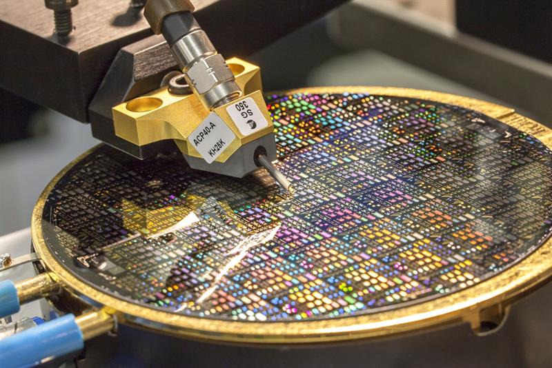
| Above: A team of researchers at Fraunhofer IAF has been working on the piezoelectric properties of ScAlN for the use in high-frequency filters for many years. The picture shows the characterisation of such devices on a wafer. |
 One of the biggest challenges of the project is growing the crystals. The project team needs to develop new techniques to accomplish this during the next months in order to reach reproducible results and to produce layer structures that can successfully be used for power electronic applications.
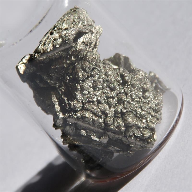
| Above: Pure scandium |


