P-N junctions created using graphene
1 min read
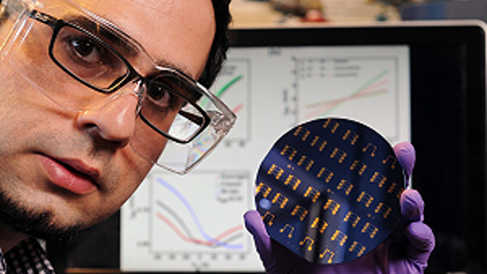
Researchers at Georgia Tech have developed a low temperature, controllable and stable way to dope graphene films using self assembled monolayers.

This approach has allowed the team to create p-n junctions without damaging the material's lattice structure or reducing its electron/hole mobility significantly.
Graphene was grown on a copper film using chemical vapour deposition, then transferred to silicon dioxide substrates.
"We have been successful at showing that you can make fairly well doped p-type and n-type graphene controllably by patterning the underlying monolayer instead of modifying the graphene directly," said Georgia Tech professor Clifford Henderson. "Putting graphene on top of self assembled monolayers uses the effect of electron donation or electron withdrawal from underneath the graphene to modify the material's electronic properties."
The electronic properties of graphene films are directly affected by the characteristics of the substrates on which they are grown or to which they are transferred.
"Any time you put graphene into contact with a substrate of any kind, the material has an inherent tendency to change its electrical properties," Prof Henderson said. "We wondered if we could do that in a controlled way and use it to our advantage to make the material predominately n-type or p-type."


