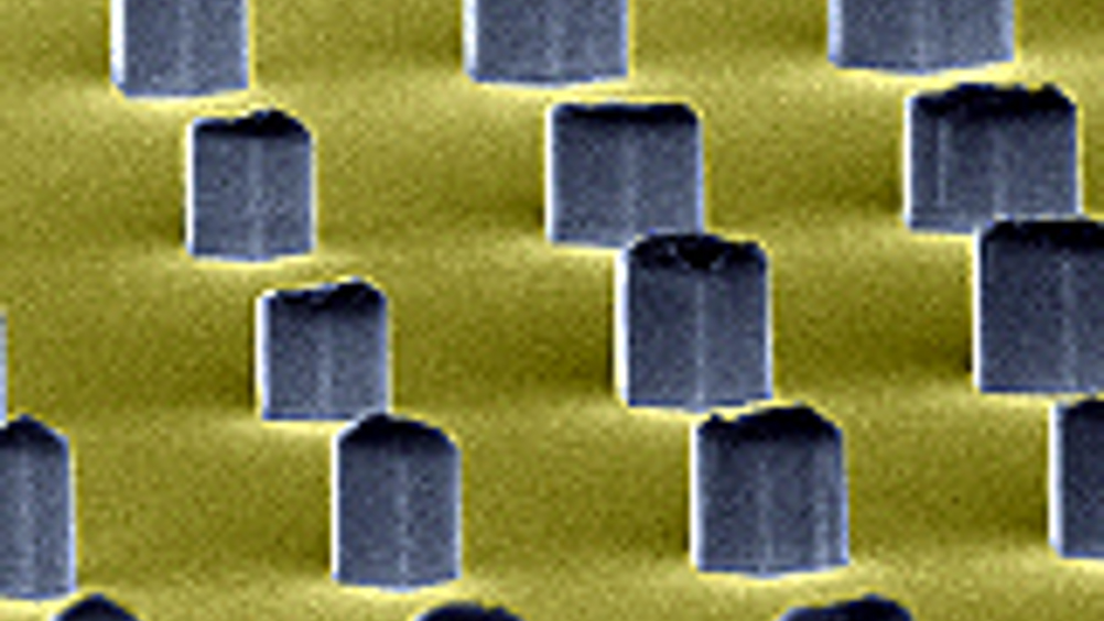
NIST researchers grow semiconductor nanowires reliably
1 min read
Researchers at the US National Institute of Standards and Technology (NIST) have cultivated thousands of nanocrystals in what is described as a step toward 'reliable mass production of semiconductor nanowires' for use in such devices as sensors and lasers.
NIST researchers grew nanowires made of gallium nitride alloys by depositing atoms layer by layer on a silicon crystal under high vacuum.

The key trick, said the researchers, was to grow the wires through precisely defined holes in a stencil like mask covering the silicon wafer. The nanowires were grown through openings in patterned silicon nitride masks and some 30,000 nanowires were grown on each 76mm diameter wafer. Wires were said to have grown uniformly through most openings and to have been absent on most of the mask surface.
Mask openings ranged from 300 to 1000nm, in increments of 100nm. In each 300nm or 400nm opening, a single nanowire grew with a well formed hexagonal shape and a symmetrical tip with six facets. Larger openings, however, produced more variable results. Openings of 400nm to 900nm yielded single crystal nanowires with multifaceted tops. Structures grown in 1000nm openings appeared to be multiple wires stuck together. All nanowires grew to about 1000nm in height over three days.


