
“Novel computing paradigms are needed to keep up with the demand for faster, smaller and more energy-efficient devices,” said Gina Adam, pictured, a postdoctoral researcher at UCSB’s Department of Electrical and Computer Engineering. “In a regular computer, data processing and memory storage are separated, which slows down computation. Processing data directly inside a 3D memory structure would allow more data to be stored and processed much faster.”
In 1959, the physicist Richard Feynman spoke of a future in which tiny machines could perform huge feats – and the challenges as he presented them at the time have been met. However, a nanoscale 8bit adder operating in 50 x 50 x 50nm volume, put forth by the Foresight Institute as part of the current Feynman Grand Prize challenge, has not yet been achieved.
But, said Professor Dmitri Strukov from UCSB, the continuing development and fabrication of progressively smaller components is bringing this size of computing device closer to reality. “Our contribution is that we improved the specific features of that logic and designed it so it could be built in three dimensions.”
Key to the development is said to be the use of a logic system called material implication logic, combined with memristors. Unlike conventional computing logic and circuitry, logic operation and information storage happen simultaneously and locally in this format. This reduces the need for components and space typically used to perform logic operations and to move data back and forth between operation and memory storage. The result of the computation is immediately stored in a memory element, which prevents data loss in the event of power outages.
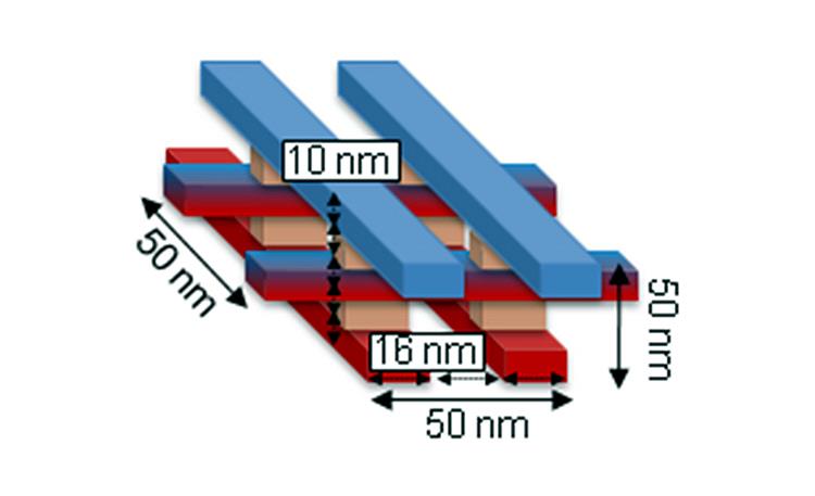
In addition, the researchers reconfigured the memristor into a 3D block, which could then be stacked and packed into the space required to meet the Feynman Grand Prize Challenge.
“Previous groups show that individual blocks can be scaled to very small dimensions – let’s say 10 x 10nm,” said Prof Strukov. By applying those results to his group’s developments, he said, the challenge could easily be met.
“Since this technology is still new, more research is needed to increase its reliability and lifetime and to demonstrate large scale 3D circuits tightly packed in tens or hundreds of layers,” Adam said.


