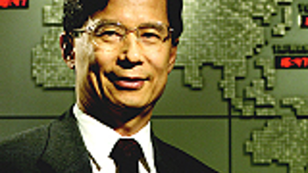
Jack Sun, vp R&D, TSMC
1 min read
Europe is becoming increasingly important to TSMC, according to Jack Sun the company's vp for R&D.

"We're expanding the R&D work we're doing in Europe," he noted, "and are trying to attract top talent to the team."
The expansion of European R&D is seen by Sun as a natural progression. "We've been a core member of the IMEC research programme for many years and have had a joint research relationship with NXP for a couple of years."
Sun talked to New Electronics during a break in the company's latest seminar in Amsterdam. Sun described the turnout of around 250 people as 'good'. "The attendance was quite broad and it was very significant that people flew in from all over Europe. It shows the industry is still interested in the future."
He claimed TSMC is investing heavily during the downturn so its customers can 'come out winning'. "We're expanding R&D to cover two more areas," he continued, "special derivatives, such as analogue, high voltage and embedded flash, and integrated packaging."
R&D is now focused in three main areas, Sun noted, with staffing increased by 30% to cover the new work. Included in this is a 15% boost in the number of people doing design R&D. "They are working on foundation library and IP development and on enabling the design flow."
TSMC is also developing its Open Innovation Platform approach
A key element of the Open Innovation Platform is a set of ecosystem interfaces and collaborative components initiated and supported by TSMC that empowers innovation more efficiently throughout the supply chain and which enables the creation and sharing of value.
"The innovation platform provides a foundation that our ecosystem partners can contribute to and which gives TSMC an assurance of IP quality," said Sun. "The platform allows everyone to collaborate, because we all have to maximise profit and eliminate waste."
Meanwhile, lithography remains high on the R&D list. Sun said that immersion lithography continues to work well and will be used at the 28nm node. "But beyond that," he continued, "we may have to resort to double patterning. However, e-beam and extreme ultraviolet (euv) will also be important."
Sun said progress had been made with euv and that TSMC's assessment is that it will coexist with the other approaches, with 'each providing something'. "But industry will have to cooperate and innovate in order to overcome the cost challenges of euv and e-beam."
TSMC will be qualifying its 28nm low power process in Q1 2010 and this will be followed in the next quarter by the high power variant.


