
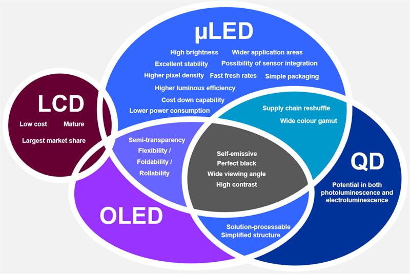
OLED had the allure of a much better contrast ratio as black really could be guaranteed to be black. The organic molecules that act as the light emitters can be printed onto flexible substrates, implying a lower cost of production once optimised and pointing to displays that the user could roll up to transport.
Although flexible displays have come to market as promised, OLEDs face some continuing issues such as production yield and lifetime. Consumers have complained about burn-in problems on large TVs and relatively low yields have kept prices high. While they try to improve OLED yields higher-end manufacturers are keen to find an alternative to conventional LCD panels.
Analysts, IDTechEx, point to the migration of manufacturing from countries such as Japan, Korea and Taiwan that have dominated the market for decades to mainland China. Those established manufacturers have either moved production into China to compete with the new crop of suppliers based there or are switching to technologies that might offer better margins in the medium term.
One possibility lies in the improvement of LCD technology involving a move to quantum dots. These fluorescent chemical combinations can offer greater contrast when fed by a backlight compared to the colour filters of classic LEDs.
Though companies continue to explore quantum-dot technology, a more promising near-term option looks to the miniLED backlight. This uses many thousands of LEDs, each 1mm across or smaller, spread across the backplane to illuminate the panel in place of the much more coarse-grained structure used in traditional panels. This incurs a higher cost because of the pick-and-place operations needed to assemble the backplane, but the advantage is fine-grained control over image contrast and with it a quality that approaches OLED.
Display Supply Chain Consultants (DSCC) has estimated the backlight assembly cost accounts for two-thirds of the overall cost of a 65in miniLED panel for TVs. Yet, it is only slightly more expensive to produce than a comparable OLED panel. The original attraction of OLED technology lay in its apparent ability to benefit from large-area printing techniques: potentially delivering TV-size screens from the end of a roll.
Rapid improvements in assembly technology could come as more money piles into an even smaller successor to the miniLED. By bringing the size down to sub 100µm levels, the microLED makes it possible to dispense with the LCD overlay entirely and move to an entirely emissive display, just like an OLED panels. The drawback is the need to assemble millions of unpackaged LEDs across a panel. But there is no shortage of cash trying to find an efficient answer.
Eric Virey, principal analyst for display technologies and markets at Yole Développement, says more than $5bn has already gone into microLED R&D, resulting in close to 2000 patents being filed by the end of 2020, adding: "Activity is strongly dominated by Chinese companies, followed by Korea." However, the US has a number of strong players in terms of patent grants and applications with Apple only narrowly trailing the number one in patent activity, Samsung.
Another player is Facebook, though its main interest in the technology is for the virtual-reality headsets made by its Oculus subsidiary. To give it a supply of microdisplays for those headsets, the social-media giant cut a deal to obtain the output for several years of UK specialist Plessey Semiconductors. A key difference with the VR form of microdisplay is that the microLEDs do not need to be diced and reassembled on a panel. They are similar in size to the image sensors used in high-end digital cameras. In the case of the technology developed by Plessey, the array of microLEDs is transferred as one large chip and bonded to a driver panel.
In the early stages of microLED development, producing the LED structures in high yield to begin with was the main focus of attention. Initially, the technology relied on sapphire wafers but manufacturers such as Aledia and Plessey demonstrated that silicon is viable. The gallium nitride (GaN) materials used favour blue light rather than any other. However, quantum dots or other fluorescent materials can convert the blue light to red or green. Because the conversion efficiency is better for red than for green, Plessey developed a native green GaN emitter.
Assembly process
Now R&D attention is shifting to the assembly process, which may feed into production based on both miniLEDs and microLEDs.
There are no clear winners right now and equipment suppliers have come up with a range of options, ranging from trying to reduce the total number of placement operations by first packaging RGB elements into prefabbed pixels to the use of microfluidics to float the elements into substrates that have been stamped with a template.
Today's leading contenders look to be a refinement of existing pick-and-place technologies and novel laser-based processes being explored by manufacturers ranging from laser 3D-Micromac to Intel, where pulses from a UV laser separate individual elements from the wafer so they can drop onto a carrier that stamps the microLEDs into place on the target.
3D-Micromac claims its laser transfer technique can process 130 million elements an hour.
Test is another challenge. Ideally, the process would check the individual LEDs work on the wafer before conveying them to the placement stage. But as with conventional chip testing, wafer probing is extremely difficult to perform reliably, which may mean finding a way to test microLEDs after lift-off but before they are placed or simply accept that repair of individual pixels after placement will be necessary, which could be costly in itself if the industry cannot find efficient ways to remove dud pixels and replace them.
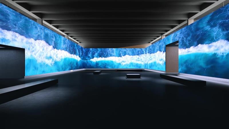
The relative complexity of microLED assembly points to it being isolated to high-end applications in the near term. An example being a giant screen made by Sony and unveiled at cosmetics company Shiseido's research centre in Yokohama, Japan. Measuring 19.2 x 5.4m, Sony made the 16Kx4K using modules but which do not suffer from the obvious joins of other display technologies: miniLEDs and microLEDs can be placed right up to the edge of each unit.
Large and modular displays for custom applications that can absorb the cost of precision assembly provide a path to commercialisation and another advantage of larger displays in areas such as signage is that they can use the larger miniLED-scale components.
Signage users will also avoid a problem microLED manufacturers need to address. In theory, the brightness of microLEDs should be better than that of OLEDs but miniaturisation lowers their effective quantum efficiency (EQE). A large blue LEDs can hit an EQE of 70 per cent but this can drop as low as 20 per cent for microLEDs.
Even assuming assembly costs come down, some sectors may still be an uphill struggle for microLEDs against entrenched technologies. Smartphones are often replaced on a two or three-year cadence, which reduces the impetus to find displays that promise significantly longer service lifetimes compared to TVs and public signs.
OLED producers may feel even safer in the smartphone and tablet markets because, as the cost of assembly is dominated by the number of pixels rather than panel size, an ultra-high resolution microLED display for a smartphone will not be that much cheaper to make than a significantly larger laptop or TV screen at the same resolution.
Much depends on how assembly techniques are optimised but until that is clear, it will be hard to predict whether OLED or microLED will dominate the high-resolution display industry.


