
Clocks are the heartbeats of embedded systems, providing timing references and synchronisation between components, subsystems, and entire systems. Excessive jitter in clock signals can significantly degrade system operation.
Fundamentally, jitter is any unwanted deviation in signal edge timing from where it should be. Jitter is a fact of life in the design of embedded systems and communication links. As such, for systems to operate reliably under a broad range of conditions, thorough characterisation of jitter is a must.
Understanding all there is to know about jitter is not for the faint of heart. Fortunately, modern digital oscilloscopes are making timing and jitter measurements almost routine, as the following examples will show.
Clock jitter characterisation
Modern oscilloscopes support a range of measurements that provide a good starting point for jitter analysis and to verify that the clock frequency is meeting specifications. The use of measurement statistics functions, such as minimum and maximum frequency, are useful for ensuring that the clock frequency is within tolerance, while standard deviation provides a quantitative measure of frequency stability.
However, measurement statistics by themselves give little insight into the manner of frequency variation. That’s where graphical tools such as measurement histograms come in to give more information about the characteristics of the various measurement variations.
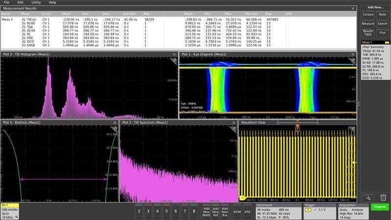
Take a 40MHz clock example, the jitter summary measurement result shown in Figure 1 includes an eye diagram of the signal, plots showing the histogram and spectrum of the TIE measurement, and a decomposition of the jitter into its individual components.
At first glance, the open eye in the eye diagram suggests that the clock signal has fairly low jitter. Indeed, the Total Jitter (TJ@BER) measurement value of about 554ps is about 2.2% of the 40MHz clock period. The jitter decomposition shows that the Random Jitter (RJ) component is a very small part of the total jitter.
Therefore, the Deterministic Jitter (DJ) must be the dominant component. The bi-modal nature of the TIE histogram also suggests a strong deterministic jitter component. The DJ is further decomposed into Periodic Jitter (PJ), Data Dependent Jitter (DDJ), and Duty Cycle Distortion (DCD).
The PJ here is about a quarter of the jitter. There are clear spectral components in the TIE Spectrum plot, indicating strong peaks at 7, 17, and 32MHz, which suggests that the jitter has significant uncorrelated DJ, perhaps caused by signal crosstalk on the circuit board or within the FPGA. Since this is a clock signal rather than a data signal, the DDJ is zero. The DCD also makes up about a fifth of the total jitter, suggesting that the clock shaping circuit deserves further analysis and optimisation.
| The above shows the impact of jitter at the transmitter on self-clocking buses, such as CAN |
Low-speed serial bus jitter measurements
Jitter also affects the performance of serial buses including self-clocking buses. Figure 2 shows an analysis of a 500kb/s differential CAN bus signal at the transmitter. Similar measurement techniques can be used on other serial buses, at the transmitter and the receiver.
The first step in this analysis is to recover a clock signal from the serial data signal. In this case, the oscilloscope is performing a clock recovery using a Phase Locked Loop (PLL) with a narrow loop bandwidth to remain locked between data bursts. This recovered clock is then used as the reference for the jitter analysis.
Jitter decomposition shows that the majority of the total jitter at the transmitter is due to DDJ, and the random and duty cycle dependent components are very small. There is also a considerable PJ component which appears to be related to the amplitude modulation of the signal at the beginning of each of the data bursts (but not related to the individual data bits), which is visible in the eye diagram and time-domain displays.
Clocked data jitter measurements
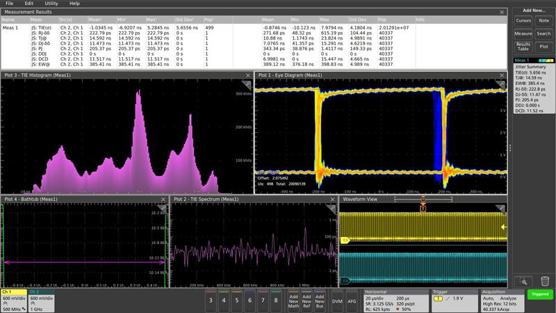
The final example that we will look at of jitter analysis is on a synchronous logic circuit. Unlike the previous examples, this circuit has an explicit clock signal, so the jitter measurements are made on the cyan data signal on channel 2 relative to the yellow clock signal on channel 1 as shown in the lower right corner of Figure 3.
The clock rate is just 1.25MHz and the circuit board traces are short, so the signals are fairly clean, as indicated by the low random jitter and wide eye pattern. Because this circuit is using a separate clock signal, the jitter typically would not be data-dependent.
In this case, the jitter seems to be dominated by duty cycle distortion. Not coincidentally, a significant portion of this circuit’s total jitter is due to the duty cycle distortion of the clock signal.
As the heartbeat of embedded systems, clocks are critical to maintaining timing references and synchronisation across components, subsystems and entire systems. As these examples of measurements on non-modulated clocks, spread spectrum clocks, serial data with embedded clock, and clocked data have shown, modern oscilloscopes offer a broad set of measurements that take the mystery out of characterising and verifying jitter in embedded systems.
| Below: Jitter analysis of a synchronous logic circuit shows how duty cycle distortion on clock circuit impacts other circuits in a system |
| Author details Lee Morgan is a Market Development Manager with Tektronix UK |


