
Looking to help designers address the market for for LED streetlights, high bay lights and other high power LED lighting applications, Power Integrations has released a reference design that claims to reduce component count and size, whilst improving efficiency and reliability.
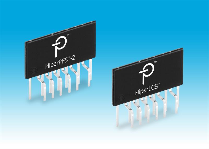
The reference design, called RDR-382, describes a constant current 43V nominal power supply for solid state lighting that delivers a 150W output from an input voltage in the range from 90 to 265V AC. The design uses the company's HiperPFS-2 PFC controller IC, as well as its HiperLCS integrated LLC power stage IC. The supply can be used to drive single or multiple LED strings and allows analogue dimming to be implemented using a 0 to 10V DC input.
The HiperPFS family comprises integrated ICs that provide active power factor correction for switching power supplies. The devices enable the design of power factor corrected rectifier front ends for switching power supplies rated at up to 425W for universal input applications and up to 900W for supplies with a 230V AC input. The HiperPFS family enables circuits that are easy to design, whilst improving design reliability via features such as input undervoltage protection, built-in overload protection and hysteretic thermal shutdown protection.
The HiperLCS family combines an LLC (two inductors and a capacitor) controller, a low and a high side driver and two half-bridge MOSFETs in one package.
Andrew Smith, the company's senior product marketing manager, noted: "Reliability is especially important for high power lighting applications with outputs of more than 75W. Because this design is high efficiency, less heat is generated. In combination with a reduced component count, this ensures a long lifetime."
Traditional dual stage drivers with separate PFC and LLC stages are said by the company to produce a constant voltage output requiring multiple DC/DC converters to create a constant current output. In contrast, it claims, the RDR-382 reference design uses a novel feedback and control scheme which enables the LLC to provide constant current directly at the output.
In this way, component count is said to be cut by approximately 30%, whilst efficiency is increased to at least 93%. Meanwhile, the elimination of the DC/DC converter stage reduces product size. A further contribution to size reduction is made by the nominal LLC switching frequency of 259kHz requiring smaller magnetics, while the use of a continuous conduction mode, variable frequency PFC stage reduces EMI compared to a fixed frequency approach, the company adds.
The design is based on the PFS7326H HiperPFS device for the PFC front end and the LCS702HG member of the HiperLCS range for the LLC output stage.
The front end of the design comprises: an input filter and boost converter; EMI filtering and inrush limiting; the main PFC stage; and a primary bias supply.
In the EMI filtering stage, two capacitors (470nF and 220nF, both 275V) are used to control differential noise, while a 4.7? 2W wire wound resistor is used for damping, improving the power factor and reducing EMI.
Two further 680k? resistors discharge C1 and C2 when AC power is removed, whilst a 2.5? NTC thermistor provides inrush limiting. A 2.2nF ceramic capacitor filters common mode EMI, whilst a 150µH inductor filters differential mode EMI.
In the main PFC stage, a selection of resistors provides output voltage feedback, whilst a capacitor provides fast dv/dt feedback to the PFS7326H's feedback pin. This allows the section to handle the PFC circuit's response to rapid undershoot and overshoot. Meanwhile, frequency compensation is provided by two capacitors (2.2µF, 25V and 47nF, 50V) and three resistors (6.2k?, 487k? and 3k?). Three further resistors, filtered by a 22nF capacitor, provide input voltage information to the PFS7326H.
In the LLC converter stage, the half bridge output of the LCS702HG drives a transformer via a blocking/resonating capacitor rated at 8.2nF, 1000V. The capacitor value was selected for the output ripple current and to withstand the high voltages which may occur during a fault.
The transformer, designed to have a leakage inductance of 49µH, in conjunction with the capacitor sets the primary series resonant frequency at 259kHz. According to the company, this value was found to be an acceptable compromise between transformer size, output filter capacitance and efficiency. A further benefit of this frequency is that it allows the use of ceramic and film capacitors.
The transformer's output is rectified and filtered by a 150V, 20A Schottky diode, selected for high efficiency, and two 4.7µF, 63V polyester dielectric capacitors. Intertwining the transformer secondary halves is said to reduce the worst case peak inverse voltage and to therefore allow the use of the Schottky diode. Additional output filtering is provided by an inductor and a capacitor, which also damps the LLC output impedance peak.
The output current is sensed via two 0.1? 2W resistors clamped by a 100V, 1A diode. This is said to avoid damage to the current control circuitry during an output short circuit. A resistor and a Zener shunt provide a voltage reference to an op amp used as a current sense amplifier. The voltage from the current sense resistor is applied to the non-inverting input of the op amp, which drives an optocoupler.
A further Zener diode and a 10k? resistor provide output voltage sensing to protect the power supply in case the output load is removed. Selecting a 10k? resistor and a 39V Zener diode is said to provide a soft voltage limiting characteristic that helps to prevent oscillation at the knee of the V-I curve and improves the supply's start up characteristics into the specified LED load.
Meanwhile, a remote dimming capability is provided by a circuit element comprising two transistors, a selection of resistors and a 100nF, 50V ceramic capacitor. A dimming voltage applied to the circuit is converted to a current by two 24.9k? resistors and applied to a further resistor via a current mirror.This current pulls down on the reference voltage to the current sense amplifier and reduces the programmed output current. A dimming voltage of 0 to 10V DC provides an output current range of 100% at 0V to approximately 20% at 10V DC.
The RDR-382 reference design comes with a complete description of the LED power supply, along with schematics of the PFC and LLC stages, a complete bill of materials and top and bottom PCB layouts. Information is provided on testing the supply and mechanical drawings are included which guide engineers on the construction of primary and secondary heat sink assemblies.


