
Machine vision (MV) systems usually comprise of cameras that are deployed to capture, interpret and signal a control system that has been set up to some pre-determined tolerance or to meet some specific requirement.
“We are seeing big growth in the use of machine vision, driven by advances in camera, sensor and video interface technologies and by the concept of the smart factory,” says Stefano Zammattio, product manager, Intel Programmable Solutions Group.“The cost of implementation is coming down and this technology improves overall levels of reliability and quality significantly.
“As with most industrial markets, there is pressure for greater connectivity – customers want one control system to run a production line – and machine vision technologies have tended to use older types of connectivity solutions that use a lot of bandwidth and are expensive to deploy and manage.
“More often than not, you have to provide a custom solution, so the drive is to not only improve performance, but also to do so at lower cost. Camera manufacturers want to be able to add or subtract functionality and tweak quality and performance.”
Vision is becoming more sophisticated. Traditionally, the requirements tended to be simple – identifying a colour, for example – and then making a decision determined by that colour. Today, the complexity of the products being monitored, along with increased volumes and the need to analyse, process and make decisions in real time, requires much greater intelligence. There is also a growing, if still niche, interest in areas such as 3D imaging and material and textual analysis.
As a result pressure is growing on all aspects of the MV system starting from the image sensor right the way through to the image processing, compression, video format conversion, connectivity and storage.
“With the deployment of HD display resolution, the need to refresh at 60frame/s becoming standard and High Dynamic Range becoming increasingly popular, there is a need to process large quantities of data in real time so as to avoid latency between the physical scene and the processed image,” explains Zammattio.
Sensor manufacturers are using a variety of electrical interfaces to output pixel information from their sensors and the resulting complexity can cause processing problems for designs based on ASSPs, which tend to be constrained by their ability to handle only one or two sensor interfaces. As a result, this could inhibit the wider adoption of MV.
“FPGAs have an advantage in that they can be reprogrammed to accommodate different sensor interfaces. They can also support camera manufacturers looking to upgrade to improved sensors without having to redesign the camera board with a different DSP,” argues Zammattio. “They are capable of integrating a range of functions on one device; such as image capture, camera interfaces, preprocessing and communication functions.”
With entire machine vision systems possible on a single device costs, power consumption and board space can be saved.
Antonio Ciccarelli, product marketing manager, Industrial and Security Division of ON Semiconductor’s Image Sensor Group, says: “While the MV market has tended to focus on frame rate, the industrial market is dependent on throughput for quality inspections. So this means the image sensor’s throughput is a key requirement, which is why more bandwidth and more processing capabilities to accommodate faster image sensors is so important. New interfaces, capable of carrying greater bandwidths, are going to be crucial.”
Numerous interfaces exist which connect cameras and computers; the most popular in the machine vision market being Camera Link, GigE Vision, USB3 Vision and CoaXPress. When deciding on which to deploy, the system designer will need to consider image throughput, cost, cable length, scalability and whether power can be supplied over the cable. In the case of CoaXPress, another decision needs to made about whether or not a frame grabber will be required.
But it’s not just greater speed that customers are asking for; they are also looking for improved image resolution to address such aspects as 3D imaging and texture analysis.
“There is constant and growing demand for finer detail images of whatever the customer is looking to inspect,” Ciccarelli explains. “When it comes to quality inspection, for example with a PCB, cameras need to be able to read the characters on components accurately; ensure they are placed on the board correctly; ensure they are oriented correctly and soldered in place. As components get smaller, cameras need higher resolution.”
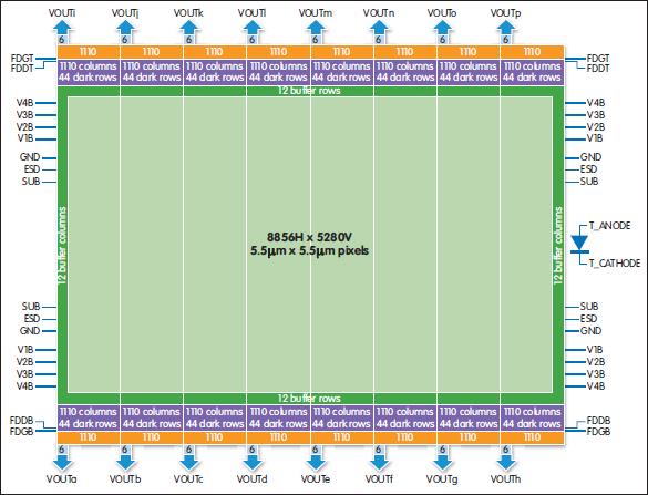
Fig 1: Block diagram of ON Semiconductor's KAI-47051 image sensor
Sensors need to be faster in order to deliver these requirements and while there has been a noticeable migration from CCD technology to CMOS, Ciccarelli offers a note of caution.
“While CMOS technology can operate at faster frame rates, not all applications will benefit from this technology. It’s important that you offer to match the most appropriate technology with the needs of different applications. Remember that a lot of this technology is being developed to augment human activities.”
CCD and CMOS images are the two technologies used to capture images digitally. Each has advantages; with CCD, for example, each pixel’s charge is transferred through a limited number of output nodes, converted to voltage, buffered and then sent off-chip as an analogue signal. As all the pixel can be devoted to light capture, image uniformity is high, providing much better quality than tends to be the case with CMOS.
CMOS chips tend to be more complex and have less space for light capture. But as each pixel performs its own conversion, it is massively parallel, meaning that bandwidth is higher.
“As each pixel in a CMOS device has its own amplifier, there can be a problem with noise, while pixel to pixel variations can cause problems,” Ciccarelli notes. However, he suggests that the cost of manufacturing CCD and CMOS imagers is not a problem. “Costs are very similar as you are not dealing with large numbers, so the benefits of mass production, associated with consumer devices do not come into play in the industrial space.”
On Semiconductor has recently released a 47Mpixel image sensor which has increased significantly the resolution available for applications such as end of line flat panel inspection.
In addition to providing higher resolution through a larger optical format, the KAI-47051 sensor (see fig 1) incorporates a reduced noise amplifier that lowers read noise while increasing dynamic range to 66dB. A 16 output architecture enables a maximum rate of 7frame/s.
“End customers will need some handholding and they will need to talk to a camera manufacturer or an inspection system integrator to identify the correct product for their application. And, as cameras themselves see more intelligence being built into them, that will raise further issues around both power and heat dissipation.
“A hotter interior will see electronics running noisier,” Ciccarelli concludes, ”and your design will need to take that into account.”


