As manufacturing systems become more intelligent – perhaps as the concepts behind Industry 4.0 become adopted more broadly – the need for more capable vision systems has grown sharply.
Machine vision systems use images to gather information on a system or process and to then make decisions based on the images captured. While such systems are dependent upon lighting and software, the camera – and the image sensor within it – is the key component in the overall operation of the system, as well as its ability to improve manufacturing quality or increase productivity.
At a high-level, a typical machine vision application involves some combination of basic measurement, counting or inspection functions. Objects may be assessed to confirm the number of objects present, to determine the number and size of features or their quality level.

So machine vision could be used to not only determine that the proper number of holes have been drilled into an item, but also to verify the spacing and shape of each hole. Similarly, the location of an object may be determined in order for it to be picked up by a robot arm or to determine whether a feature is in the correct place. Other functions include reading a barcode, performing character recognition or measuring the level of a fluid.
Each of these functions drives specific characteristics required for the final camera system and, ultimately, the image sensor required for the application. Understanding the minimum quality level of the image is paramount as this determines whether the computer system analysing the image can make an accurate measurement or reach the correct conclusion. This point is critical; other features, such as frame rate, power or size, will become secondary if the images captured are not of sufficient quality for analysis and use.
Historically, machine vision systems have required CCD image sensors because of their high image quality and performance. Today, however, CMOS image sensors have jumped to the forefront for many machine vision applications. Advances in CMOS pixel design have made the imaging quality available from this platform sufficient for a variety of different end uses.
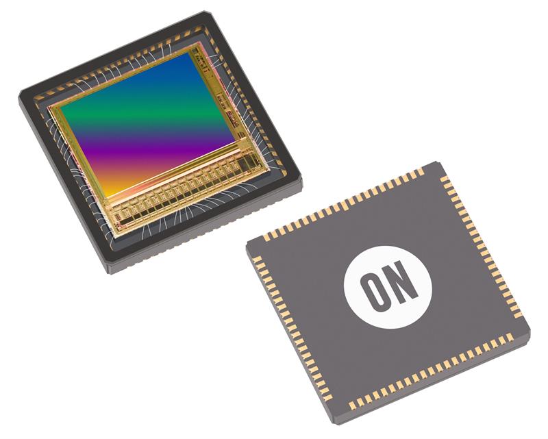
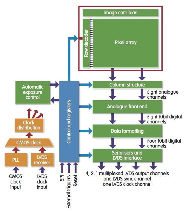
Modern CMOS image sensor platforms, such as that used in ON Semiconductor’s PYTHON family, are based on a global shutter pixel design that enables the capture of moving objects without the introduction of motion artefacts. In-pixel correlated double sampling provides low readout noise, while on-chip fixed pattern noise correction helps preserve image quality. Combined with a 10bit A/D converter and a dynamic range of 60dB, these features allow machine vision systems to leverage the intrinsic advantages of a CMOS platform in their operation.
With many machine vision applications looking to operate at ever higher speeds in order to increase productivity, image sensors must support high bandwidth readout. The output architecture of the CMOS platform enables this as additional digital outputs can be added to increase the available bandwidth. For example, the use of up to 32 separate LVDS outputs enables high resolution PYTHON devices to realise bandwidths that exceed those of modern computer interfaces, including 10Gbit Ethernet or USB 3.1. The ability to output at up to 80frame/s from a 25Mpixel device is well beyond the capabilities of standard CCD designs.
The inherent flexibility available in CMOS output designs allows the frame rate to be further increased when operating in Region of Interest (ROI) mode, where only a portion of the image sensor array is read out. With proper design considerations, the speed increase when operating in this manner can scale by both the x and y dimensions of the ROI, enabling faster frame rates than can be realised when using a more standard CMOS output design, which only scales the x dimension.
Consider the frame rates from the PYTHON 5000 image sensor compared to theoretical frame rates from a similar 5Mpixel sensor using a standard CMOS output. At full resolution, both designs would provide approximately 100frame/s, but when reading out a 1280 x 720 pixel ROI, the the PYTHON device’s frame rate increases to almost 600frame/s, while the standard output design would increase to only 300frame/s. This can be an important differentiator.
While high resolution can provide finer detail, this must be balanced by making sure that too much information is not captured, which would slow data processing. In addition to having the right number of pixels, they need to be in the appropriate aspect ratio for the application. For example, an aspect ratios of 1:1 is often used in pick and place applications to maximise image capture across the full field of view.
Different spectral sensitivities, such as colour, monochrome and extended near infrared (NIR), may also be required to optimise the imaging system for the application. In order to do this, a camera manufacturer will look for an integrated family of image sensor products that includes multiple resolution nodes and colour options to support a portfolio of products.
The PYTHON family has more than 40 options, with resolutions ranging from VGA to more than 25Mpixel. These devices are available in multiple configurations, including monochrome, Bayer Color and extended NIR sensitivities. Selected devices are available in low-power configurations or with removable tape to protect the image sensor during the camera assembly process.
To help designers understand the performance available from the PYTHON family of image sensors, Avnet Silica offers a range of evaluation kits. These kits include an image sensor, the appropriate sensor headboard, FPGA evaluation board and software and accessories. The flexible design also allows the evaluation hardware to be use with other PYTHON devices by purchasing additional image sensors.
After identifying the most appropriate image sensor, designers then need to consider the remainder of the camera design. Complementary products from ON Semiconductor include embedded boards, power and signal chain components that allow engineers to choose between modular solutions and the flexibility of a discrete design.

If a machine vision system needs to be brought to market quickly, it may not be possible to build it from the ground up. For those applications, Avnet Silica products such as the PYTHON-1300-C camera module. Based on the PYTHON 1300 colour image sensor and featuring a 0.5in SXGA CMOS image sensor with a resolution of 1280 x 1024 pixels, the module can be combined with Avnet Silica’s MicroZed Embedded Vision Carrier Card and the Smart Vision Development Kit to provide a complete hardware design, leaving the designer to only write the application software.
While CCD image sensors may still remain preferable in some specialised applications, the combination of image quality, bandwidth, imaging flexibility and configuration flexibility available from CMOS image sensors has accelerated adoption of this technology in machine vision applications.
The imaging capabilities of such devices has ushered in a new level of performance and functionality for industrial imaging and CMOS sensor based imaging is now suitable for use in almost every type of design.


