
A growing number of emerging applications, such as Head Up Displays (HUDs), AR/VR headsets and general wearables, are looking at new display technologies to enable the development of next generation products that will meet growing global demand. According to research consultancy Yole Développement, the market could reach as many as 330million units by 2025.
Although augmented and virtual reality are probably being seen consumer technologies, they are increasingly used in industrial and manufacturing applications, providing skilled and semi-skilled workers with access to information that can assist them in a range of tasks. Examples may include showing a worker the correct sequence for fixing and tightening bolts in an engine, or rivets in a larger structure such as a fuselage. When tools are also connected, the process becomes altogether more integrated, delivering quality assurance as each fixing is recorded or highlighting those that haven’t yet been secured.
Head-mounted displays not only add a level of realism to the scene, they can further increase productivity by allowing workers to move around unencumbered by large handheld displays or tablets.
Display technology is evolving in order to meet demand for smaller, lighter headsets that can be worn for an entire shift without becoming a burden or potential health hazard. The drive for more efficient displays is pushing innovative manufacturers towards microLEDs; a technology that promises lighter, smaller and more efficient displays.
Emerging applications
Headsets are one important and emerging application area for smaller displays, but others include HUDs, which are now being integrated into road vehicles. Existing applications include general wearables such as smart watches and, of course, displays have always been part of the Human-Machine Interface. This will continue, as smaller displays will allow them to be embedded within a wider range of devices.
Displays generally fall into one of two categories; reflective or emissive. Reflective displays typically require a separate light source and mirror arrangement, while emissive displays, such as LEDs, generate their own light.
Today’s headsets are often based on reflective display technology due to the lack of available emissive displays, which is why they appear large and heavy and are generally power-intensive. Moving to an emissive display solution for headsets will reduce the overall size, weight and power consumption, leading to a significant change in market dynamics.
Like other forms of emissive display technology, microLEDs feature three LEDs per pixel – red, green and blue – in order to provide the full spectrum of visible light. The name reflects the small size of each LED, often 10μm or less, on a pixel pitch of less than 40μm. While this makes them suitable for HUD applications, they can, in theory, be applied to any display of any size; scalability is one of the technology’s many benefits.
| “In simple terms, the same luminance can be achieved for much lower power – a critical parameter for the target applications.” Keith Strickland, chief technology officer, Plessey Semiconductors |
For larger displays, such as TVs, tablets or mobile phones, pixel pitch is less demanding. However, applications such as HUDs in vehicles, head-mounted displays and wearables, require pixel densities of hundreds of pixels per inch, which means the pitch shrinks significantly. In manufacturing terms, this presents challenges with respect to incumbent technologies such as OLED.
The main advantages that make microLED technology worth pursuing in the face of those technical challenges include higher luminosity; typically, an OLED produces in the region of 1000 Nit (1Nit is equal to 1candela/m2), while microLEDs can produce upwards of 100,000Nit. In simple terms, this means the same luminance can be achieved for much lower power – a critical parameter for the target applications.
Manufacturing challenges
Conceptually, manufacturing a display comprising three LEDs per pixel involves combining LED chips and an active matrix to drive each chip individually. Today, the vast majority of LEDs are manufactured using gallium arsenide (GaN) on sapphire wafers.
In display applications, each LED needs to be attached to the active matrix. However, GaN on sapphire doesn’t lend itself to integration with CMOS circuitry, so each LED chip needs to be physically placed on a silicon substrate implementing thin film transistors. In larger displays with a pixel pitch of 70μm or more, this isn’t too difficult. But as display sizes reduce and pixel pitches shrink, the manufacturing equipment becomes less efficient.
Effectively, the process involves picking the LED chips up and placing them with extreme accuracy on the silicon substrate. While the cost of developing and manufacturing the pick and place equipment is one factor, a more important question is the ability of companies to make pick and place equipment that is accurate and efficient at pixel pitches of 20μm or less.
A major concern is the yield that can be achieved, both in terms of selecting working LED chips (and removing those that do not work) and placing them accurately. Reworking a microLED display would likely be economically unviable, so the total yield will be determined by both factors.
The alternative tactic is to use a monolithic approach with multiple emitters on a single chip. This requires moving the LED manufacture to a substrate that accepts silicon more readily and the most promising technology in this respect is GaN on silicon. It provides the ability to make larger LED emitters, with better contrast, thanks to the technology’s surface-emitting properties. The technique can easily be scaled to 200mm wafers and larger, improving cost and yield.
Monolithic approach
Monolithic in this context means there is no need to use pick and place machines; LEDs are manufactured on a silicon wafer which is directly bonded to another silicon wafer containing the active matrix. Removing the need to pick and place individual LED chips means the entire process becomes much more efficient in manufacturing terms, as well as economically scalable.
This includes wafer size; sapphire wafers are typically available economically up to 6in (150mm), but silicon wafers of 200mm and 300mm are commonplace, as is the manufacturing equipment used in the fabrication of CMOS devices.
The technology and intellectual property developed by Plessey Semiconductors is attuned to the large-scale manufacture of microLEDs using GaN on Si.
The company’s background in developing CMOS sensors also lends itself to microLEDs, as much of the underlying technology is transferable. While pixels become emitters instead of sensors, a lot of the addressing technology is comparable.
Another advantage is that GaN on Si LEDs are surface-emitting devices, as opposed to GaN on sapphire, which is a volume-emitting technology. In simple terms, this means more of the light generated is emitted in the desired direction. Although a waveguide is still required, less of the light is lost due to alignment or the photon’s exit vectors, further improving the power efficiency of the display.
Current waveguide interfacing is a very lossy process with very little of the light entering a HUD usable by a viewer. Monolithic micro LED arrays could mean a transformation from typical VR headsets to something more akin to a pair of glasses.
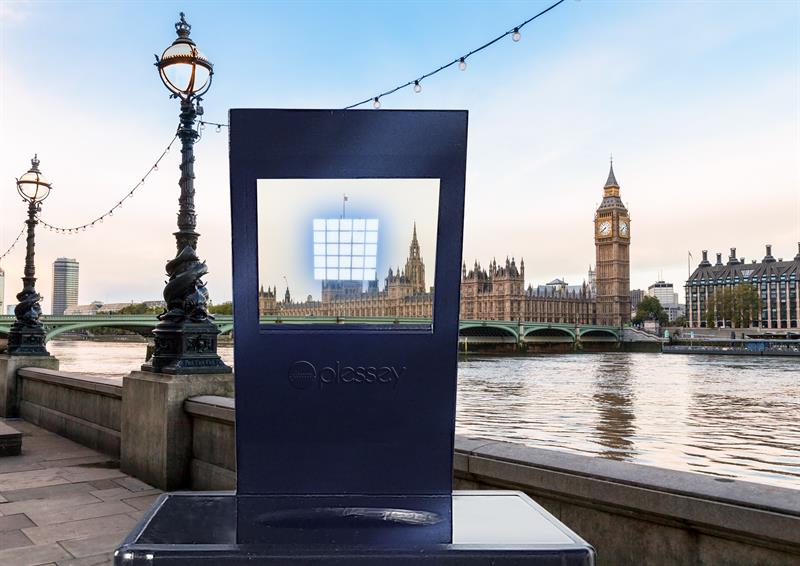
| Below: A demonstrator, produced in collaboration with Artemis Optical, features Plessey’s monolithic display, based on an array of microLEDs |
Conclusion
Demand for smaller, power-efficient displays is building, from applications including HUDs and AR/VR headsets. This will put pressure on the incumbent technologies, which will struggle to scale down to the sizes required both in practical terms and economically.
The availability of a robust GaN on Si process is now enabling the manufacture of monolithic microLED displays. This technology is proven to meet the demands of emerging display applications and is now being made available through technology licensing agreements.
As the dimensions of displays reduce, GaN on Si is emerging as the most technically and commercially viable approach to meeting demand for microLEDs that deliver high efficiency, high pixel density and low power.
Author profile: Keith Strickland is Plessey Semiconductors’ chief technology officer |


