
There was a lot going on behind the scenes then; already, Altera was talking with Intel about using its foundry service to build ‘Generation 10’ devices, eventually being acquired by Intel in 2015.
Now the first fruit of that work has appeared in the form of Stratix 10 MX. Designed to meet the needs of those developing high end communications systems, the device integrates stacked memory dice alongside an FPGA die, providing users with a memory bandwidth of up to 1Tbyte/s.
“A few years ago,” said Jordan Inkeles, director of product marketing for high end FPGAs, “we partnered with Intel for lithography and were very excited. We also looked at Intel’s packaging technology and asked ‘can we use that?’. The answer was ‘yes’. The combination has allowed us to do things we thought were not possible.”
The concept is based on what Altera – now Intel’s Programmable Systems Group (PSG) – calls ‘tiles’. Essentially, these are the dice which sit alongside the FPGA. Tiles are connected to the FPGA using Intel’s EMIB – embedded multi-interconnect bridge – technology. “It’s not a traditional silicon interposer,” Inkeles explained. “It’s a little bridge chip which is used where you need to connect two pieces of silicon.”
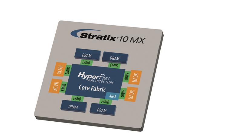
Statix 10 MX is said to combine the programmability and flexibility of STratix 10 FPGAs with integrated 3D stacked high bandwidth memory devices
Stratix 10 MX devices are designed to help engineers solve demanding memory bandwidth challenges which can’t be addressed using conventional memory solutions. The parts integrate four stacks of HBM2 DRAM, each with up to four memory dice. PSG says the parts are suitable for use where bandwidth is paramount. Apart from providing 10 times more memory bandwidth than conventional solutions, Stratix 10 MX devices are said to be smaller and to use less power.
“This idea of integrated chips opens up things,” Inkeles said. “FPGAs are trying to be everything to everyone. They have to support wireless, wired, networking, radar and high performance computing, amongst others. We saw divergence in what was possible.”
PSG started thinking about transceivers. “If we had transceivers in separate tiles, we could come out with devices for different markets,” Inkeles continued. “It also makes sense for analogue, which doesn’t move at the same pace as digital, and for design reuse. So we could use a tile that meets today’s needs – say a 28G transceiver – then come out in the future with a 56G PAM4 tile and a 28G NRZ tile. In the same process node time frame, we can deliver two very different types of product.”
This is the concept underpinning the MX. “Parallel memory is becoming a huge challenge,” Inkeles observed. “You can continue to use parallel interfaces, but with the memory right next to the FPGA to maintain signal integrity and reduce power. But, while Hybrid Memory Cube (HMC) is a good solution, it has to be serial,” he continued, “as you can’t get signal integrity on a 72bit wide datapath. Or you can put memory in the package.
“By providing up to four stacks of four DRAM dice, we’re providing a memory bandwidth never seen before. Each stack can run to 256Gbyte/s, so four stacks give 1Tbyte/s. That’s unprecedented and can’t be achieved with HMC.
“Power consumption is reduced because the memory is right next to the FPGA and drive strength is much smaller – only pJ/bit – because you’re not driving signals to a memory that could be 6in away.”
There is a downside, however; it’s an expensive solution. “You’re paying for bandwidth,” Inkeles admitted. “But customers complain about the effort it takes to do board layout and to get the DDR chips right. We’ve solved that without using any I/O or transceivers. And if 16Gbyte of DRAM in package isn’t enough, you still have transceivers and I/O available for use with external components.”
Inkeles pointed to three broad application areas for the MX device. “There’s high performance computing (HPC), cloud computing and data centres, but they all look for different things.
“HPC says ‘give me everything, while cloud says it’s worried about the cost per bit. Data centres can build algorithms in logic, which is quicker than a GPU, but need the memory bandwidth to ‘feed the beast’.”
Apart from imaging applications, such as medical and radar, Inkeles says there are applications in wireline communications. “Gone are the days of just routing traffic,” he said. “Everyone is now looking to differentiate their products, for example, by providing statistics on the data being handled. So they need to hold a piece of traffic for a moment to analyse what it is, then send it onwards. This couldn’t be done before because there wasn’t the bandwidth.”
MX is the first implementation of PSG’s strategy and the interesting thing is ‘what comes next?’. It’s quite possible that optical functionality might appear at some point in Intel PSG’s Stratix 10 parts.
Five years ago, Altera announced plans to integrate optical interfaces into its FPGAs as a way to cope with increasing communications bandwidth. Despite demonstrating the technology later in 2011, the idea remained on the shelf. Inkeles said: “We have continued to evolve the technology, but haven’t gone public with the developments.”
Inkeles noted: “Although PAM4 offers a way to stay in the electrical domain, we will, at some point, run out of capability and we’ve been preparing for that transition. Now we have transceivers on tiles, we can take out one tile and replace it with an optical interface.
“We’ve been working behind the scenes,” Inkeles continued, “but the right time to put a product into the market will depend on the economics.”
Altera’s acquisition by Intel also gives it access to silicon photonics technology. “We have exciting capabilities,” Inkeles added.
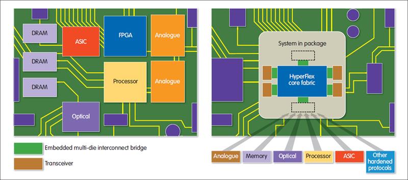 Heterogenous 3D system in package integration could enable a new class of FPGA based devices
Another potential step is integrating such components as analogue, ASICs and CPUs alongside an FPGA. Intel PSG says EMIB offers a simpler manufacturing flow by eliminating the use of through silicon vias and specialised interposers. The result, it claims, will be integrated systems in package that offer higher performance, less complexity and better signal and power integrity.
Inkeles sees this as potentially a new market. “ASICs have become smaller and faster, but not cheaper. Unless you’re going to sell millions, you will have a tough time,” he said. “ASSPs are going away, unless you can find more customers or more volume.”
Is it possible that Biran’s vision of ‘standard products’ might be close to reality and could that even include custom versions of a Stratix 10? “Will we do custom?,” Inkeles wondered. “It’s within our ability. It’s not something we’re promoting, but we are engaging with customers.
“We have a range of options. Now we’re part of Intel, the ‘sky’s the limit’. As Altera, we developed HardCopy and had an ASIC team, but it wasn’t our core competence. But Intel Foundry can do ASIC,” he concluded.


