
When things go wrong, we have to poke around the hardware, trace through the code and fix what went wrong. For a lot of designers and developers, that is the drudgery of the job.
But there are ideas and tools that can take the drudgery out of debugging; perhaps even eliminate some bugs before they even happen.
Minimising hardware debugging
Hardware components, both passive and active, are generally less the cause of functional failure than the PCB. Those components have likely been used in thousands of designs and, if interconnected and programmed correctly, will work as per specification. More often than not, it’s the tens-of-thousands of connections on dense, multilayer boards that are the source of bugs. The best way to minimise bugs is to prevent them in the first place, so here are two effective ways to help ensure the PCB works right the first time.
Design for test
Prototypes must not only be tested to determine if they meet the design specifications, but also to check if they work properly. To test the product thoroughly, there must be test points planned into the PCB design. Contacts for flying probes should be incorporated into PCB designs to allow testing of all circuitry.
However, in extremely fast circuitry, this may not be possible. In these instances, there is not enough real estate on the board to accommodate normal test points. Here are three tips for incorporating test points in dense, high speed circuitry:
- Design in a small portion of exposed copper that can be used as a test point
- Omit a small strip of solder mask at the end of a component pad for probing
- Omit the solder mask on an entire via pad so that it can be used for testing.
In this way, you can design test points into even the densest layouts. Using modern ECAD tools, you can specify these requirements within the manufacturing output files so your fabrication house knows exactly how to build your board.
Design of experiment
Products have become so complex that it is nearly impossible to test most of them exhaustively. One technique that is beginning to appear in PCB testing is called Design of Experiment, or DOE; an approach that allows a product to be evaluated within real-world operating conditions. DOE testing allows looking at cause-and-effect relationships in a controlled (or partially-controlled) way.
A set of experiments is designed to test one variable at a time while the rest are controlled. Data is collected and analysed to select the desired outcome. For example, a board layout could be simulated to determine crosstalk while trying different routes for a differential pair. The result would present the route that minimised crosstalk.
When evaluating a new fabricator, an experiment could be devised using that fabricator’s design for manufacturability (DFM) criteria to optimise a design rule set that matched their requirements.
In a more physical example, a manufacturer might devise an experiment to test a variety of solder powders; another might modify the flux. The result is the ideal combination of solder and flux to achieve the goal defined initially. The typical DOE workflow is illustrated in Figure 1.
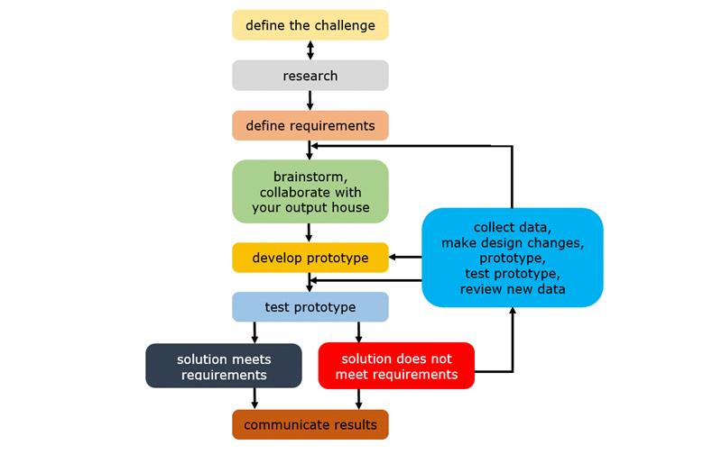 Figure 1: A typical design of experiment workflow
The DOE process can also be used to find other potential PCB problems. Imagine a board design that is so dense that there is no room for thieving (ground pouring) to help dissipate the heat generated by all those components in such close proximity. Using DOE to collect data on thermal characteristics, given a set of variables, can allow you to understand the behaviour early so that you can design around problems before they occur.
There are numerous examples in which using the DOE approach allows correct decisions to be made empirically, potentially saving a lot of time and cost by eliminating lengthy debugging using prototypes.
Software debugging
Debugging software is another problem altogether. The DOE process does not lend itself well to finding software bugs, although it could be used to analyse behaviour of different code designed for the same purpose.
In a typical software design process, the code is flashed onto the target hardware and a rich-featured debugger/emulator allows engineers to observe the code as it runs, step through, trace and locate anomalies so that the code can be fixed to perform as required. These debuggers are rather expensive and, as such, are generally run to detect timing problems on complete sets of tasks within an OS and feature sophisticated test probes. They also tend to be used late in the design when debugging and fixing the code can be a complex and time consuming task.
A debugger on every desk
While the system-level debug must still be done in order to find problems that only manifest in the complete environment, less expensive streamlined debuggers are being introduced that virtually allow a debugger to be on every designer’s desktop. These debuggers also incorporate inexpensive probes and allow the use of software simulators. The advantages are many, especially when coding for multicore architectures.
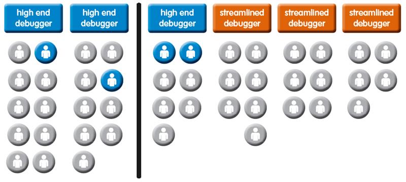
In a typical development environment, high end debuggers become limiting resources, with developers having to queue to use the tool. Using one high end debugger and adding three streamlined debuggers – for the same cost – allows developers who don't need the high end features to access debuggers more quickly
Debugging your code ‘as you write it’ with a streamlined debugger allows the functionality to be checked at any time. Much like running simulations on a portion of a PCB as it is laid out, the incremental debugging of code as it is written allows more pristine code to be integrated into the systems environment and is likely to result in fewer system problems.
These desktop debuggers allow engineers access to the most common features so that functional components can be run and evaluated. These debuggers commonly include commonly used functions such as:
- Step-by-Step execution of source code
- Step-by-Step execution in disassembly
- Configurable breakpoints
- Run to breakpoint
- Inspect and modify target, including
- Core registers
- Memory
- Evaluation of expressions
- Control of debugger with scripting
- Use of run-time libraries
- Limited tracing
Another advantage of having a debugger at each desk is coding efficiency. When the software doesn’t execute the intended function, the developer is removed from the creative thought process of coding and thrown into an ‘investigative’ mode. Returning to coding after lengthy debugging requires time to get ‘back on track’ and almost every software developer has experienced this. Fixing small bugs takes a small amount of time and allows the designer to get back to coding quickly.
Conclusion
Whether you are debugging hardware or software in embedded systems, the most efficient technique is to adopt tools and methodologies that allow errors to be recognised and rectified as close to ‘when made’ as possible. This results in least cost, least time investment and continuous innovation from designers. The few tips outlined in this article could bring a significant improvement in product design efficiency. Give them a try!
Author profiles:
David Marrakchi is a technical marketing engineer with Altium. Dr Alexander Herz is head of product engineering with Altium Tasking.


